

An AI-enabled machine vision reader identifies difficult wafer markings across semiconductor manufacturing lines, helping reduce production stoppages, improve traceability, and maintain throughput during advanced chip fabrication and packaging.
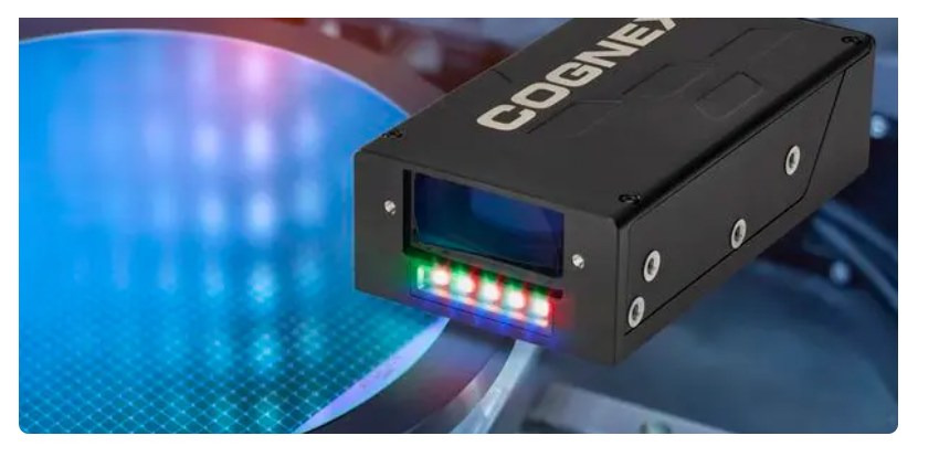
The In-Sight 1750 Series wafer and panel reader by Cognex Corporation combines edge AI, advanced imaging, and specialised illumination to identify semiconductor wafers with faint, damaged, or difficult-to-read identification marks. Developed by Cognex, the system is designed to reduce manufacturing interruptions and improve traceability as chipmakers scale production for artificial intelligence (AI) infrastructure, advanced computing, and next-generation electronics.
Wafer identification is essential for tracking semiconductor materials through fabrication and packaging. When a reader cannot decode a wafer ID, production equipment may require operator intervention, interrupting automated workflows and reducing equipment utilisation. These challenges increase when markings become degraded during processing or when reflective and low-contrast substrates make identification more difficult.
The In-Sight 1750 addresses these problems by combining AI-based recognition with established reading techniques and purpose-built lighting. Its imaging system captures wafer markings, while the reader processes them to identify IDs under challenging conditions. The platform is designed to support consistent identification across semiconductor manufacturing environments, helping operators maintain production flow without relying as frequently on manual troubleshooting.
The key features are:

- Sensor resolution: 1896 × 960 pixels.
- Field of view: 38mm-wide imaging area.
- Substrate compatibility: Silicon, gallium nitride, silicon carbide, sapphire, and glass.
- AI Autotune: Automatically adapts reading and illumination settings.
- Reading methods: Edge AI OCR, conventional OCR, and Data Matrix decoding.
The product family includes two configurations. The In-Sight 1751 uses red LED illumination and RGB low-angle lighting, allowing manufacturers to select lighting conditions suited to different surfaces. The In-Sight 1752 uses infrared LED illumination for applications requiring infrared-based imaging. Both models offer a resolution of 1896 × 960 pixels, with a variable working distance.
The reader also supports a web-based configuration interface to simplify setup and includes built-in read logging for quality monitoring and process control. Manufacturers using the previous In-Sight 1740 series can convert existing jobs to the newer platform, helping simplify upgrades without extensive redesign of established installations.
Applications include wafer tracking during chip fabrication, identification of substrates in advanced packaging lines, and automated production environments where reliable material identification is critical. By reducing missed reads and the associated need for operator intervention, the system can help semiconductor manufacturers improve throughput while maintaining traceability as production volumes increase.
Click here for the original announcement.