

A carbon film developed by researchers could replace two chip wiring layers, reducing space constraints while improving electrical and thermal performance in advanced semiconductor designs.
Researchers at the National University of Singapore (NUS) have developed an amorphous carbon film that could replace two layers in future chip wiring. The material is also being evaluated with TSMC for ultra-low-k insulation and chipmaking applications, according to the source.
At just 0.8 nanometres thick, the carbon film is designed to address challenges created as transistors and their connecting wires continue to shrink. Narrower copper wires have higher electrical resistance, while smaller gaps between neighbouring wires increase the risk of electrical leakage and interference.
The researchers say the film can serve two functions within the same layer: providing low electrical resistance while also acting as a barrier that helps prevent copper from migrating into surrounding insulating material. This could reduce the need for separate barrier layers and free additional space for copper wiring.
In accelerated testing, the 0.8-nanometre film prevented copper from passing through it. Its projected time to failure at typical operating electric fields was more than 100 times the industry benchmark for a 10-year service life, according to the source.
The material also demonstrated strong insulating properties, withstanding fields of about 28–31 megavolts per centimetre before losing its insulating capability. Its measured hardness was approximately 100 gigapascals, supporting its potential for demanding semiconductor applications.
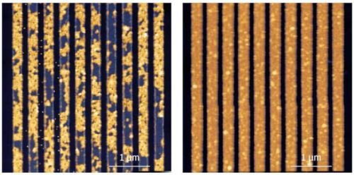
The team produced the carbon film using chemical vapour deposition, a process in which gases react on a surface to form a solid layer. The researchers report that they achieved uniform growth across a four-inch wafer and around the sidewalls and corners of patterned structures.
The work builds on earlier research into stable, freestanding monolayer amorphous carbon. NUS is now working towards semiconductor manufacturing, including further evaluation of reliability, scalability and compatibility with established manufacturing standards.