


The Space-Saving Device in the PowerPAK 1212 reduces component counts and simplifies designs by requiring 50% less PCB space than discrete devices.
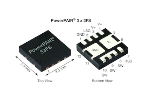
Vishay Intertechnology, Inc. has announced the launch of a new 80 V symmetric dual n-channel power MOSFET, which integrates high and low-side TrenchFET Gen IV MOSFETs into a compact 3.3 mm by 3.3 mm PowerPAIR 3x3FS package. Designed for power conversion in industrial and telecom applications, the Siliconix SiZF4800LDT enhances power density and efficiency while improving thermal performance, reducing the number of components, and streamlining designs.

This dual MOSFET offers a space-efficient alternative to two discrete devices typically used in the PowerPAK 1212 package, resulting in a 50% reduction in board space. It provides an effective solution for synchronous buck converters, point of load (POL) converters, and half- and full-bridge power stages in DC/DC converters for radio base stations, industrial motor drives, welding equipment, and power tools. The SiZF4800LDT’s high and low side MOSFETs are optimised for 50% duty cycles, and its logic level turn-on at 4.5 V simplifies driving circuits. The key features include:
- TrenchFET Gen IV power MOSFET
- Symmetric dual n-channel design
- Flip chip technology for optimal thermal management
- Industry-leading low on-resistance of 18.5 mΩ at 4.5 V, 16% and 54% lower than the closest competitor
For enhanced efficiency in high-frequency switching applications, the SiZF4800LDT boasts a low on-resistance times total gate charge — a crucial figure of merit (FOM) for MOSFETs in power conversion — of 131mΩ*nC. This low on-resistance and thermal resistance combination allows it to handle a continuous drain current of 36 A, which is 38% higher than the closest competing device. The MOSFET’s unique pin configuration facilitates a simplified PCB layout and enables shorter switching loops to reduce parasitic inductance. The MOSFET is thoroughly Rg- and UIS-tested and is both RoHS-compliant and halogen-free. They are currently available in both sample and production quantities, with a lead time of 26 weeks.