New inference hardware claims up to 10x faster AI response times with drastically lower power and cost by embedding models directly into custom silicon rather than relying on GPUs.
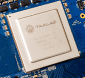
A new AI accelerator architecture by Taalas is challenging the conventional GPU-driven approach to artificial intelligence inference by converting entire AI models into dedicated silicon. The newly introduced chip architecture hardwires model weights and parameters directly into ASICs, enabling ultra-low latency and significantly lower energy consumption for large language model (LLM) inference workloads.

Unlike GPUs and even many AI accelerators that remain programmable, the new approach creates model-specific chips optimized for a single neural network. The result is dramatically faster inference performance, especially for high-volume workloads where the same AI model serves millions of queries repeatedly. According to disclosed benchmarks, the first-generation chip running a compressed Llama 3.1 8B model reportedly achieves over 14,000 to 17,000 tokens per second—far beyond most currently deployed inference hardware.
The key features are:
- Hardwires AI models directly into ASIC silicon
- Delivers over 14,000–17,000 tokens per second
- Eliminates dependence on external HBM memory
- Operates at significantly lower rack-level power
- Supports rapid chip revisions in nearly two months
The architecture removes dependence on high-bandwidth memory (HBM), one of the costliest and most supply-constrained elements in modern AI systems. Instead, model parameters are etched directly into silicon, reducing memory bottlenecks and enabling lower rack-level power consumption. The company claims AI racks based on the architecture consume roughly 12–15kW, compared to 120–600kW for GPU-based AI racks.
The system also avoids liquid cooling and advanced packaging requirements, potentially allowing deployment in standard server infrastructure. Analysts suggest this could significantly reduce infrastructure costs for cloud providers and enterprise AI deployments.
However, the tradeoff is flexibility. Since each chip is tied to a specific AI model, updates require new silicon revisions. To address this, the startup says only two metal layers need modification during redesign, allowing updated chips to be produced within roughly two months instead of years.
The company plans to scale the architecture beyond smaller LLMs toward larger reasoning models and multi-chip AI systems later this year. Industry observers see the development as part of a broader trend toward highly specialized AI hardware, similar to how TPUs transformed cloud AI acceleration.