


The smallest fully printed infrared photodetectors to date, using nanoscale printing techniques that could reshape how compact, low-cost IR sensing is integrated into next-generation electronic systems.
A research team from the University of Hong Kong has unveiled what it calls the smallest fully printed infrared photodetectors ever created, advancing room-temperature optoelectronic fabrication and pushing miniaturization beyond current silicon-centric approaches.
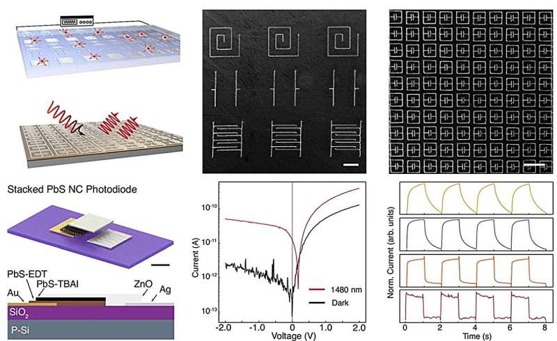
The advancement centers on an innovative nano-printing platform that integrates colloidal nanocrystal inks with high-precision patterning to produce sub-10-micrometer infrared (IR) photodiodes entirely via printing methods. This contrasts sharply with traditional IR sensors, which depend on costly growth and bonding of IR-absorbing materials onto CMOS circuits, limiting scalability and sensor footprint.
At the core of the new approach is electrohydrodynamic printing (EHDP), enhanced with a ligand-exchange surface treatment that enables extremely fine feature control including silver nanocrystal lines as narrow as 70 nm without requiring high-temperature sintering. The resulting printed films exhibit conductivities close to bulk silver, a key requirement for practical device performance.
Researchers emphasize that such precision printing at room temperature avoids damage to sensitive materials and substrates, opening avenues for layer-by-layer integration of complex, multi-material devices. The team’s demonstration marks a milestone in all-printed, sub-micrometer optoelectronics, notably shrinking IR photodetector dimensions while maintaining functional performance.

Applications for near-infrared (NIR) sensing span autonomous systems, biomedical diagnostics, and high-speed optical communications, yet conventional silicon technology inherently struggles to detect these wavelengths directly. By sidestepping silicon’s limitations and printing detectors directly with tunable nanocrystal inks, the HKU platform promises more flexible design and integration pathways.
Lead researcher Leo Tianshuo Zhao notes that colloidal nanocrystals first synthesized decades ago have long shown potential but have been bottlenecked by fabrication challenges. The team’s method finally translates that potential into practical, scalable device fabrication. Looking ahead, the team plans to apply the nano-printing technique to broader device classes, including optical metasurfaces, biosensors, and hybrid electronics, potentially reshaping how next-generation photonics components are manufactured.
