Can twistronics move beyond tiny laboratory samples? A scalable fabrication method could widen its path towards practical electronic devices.
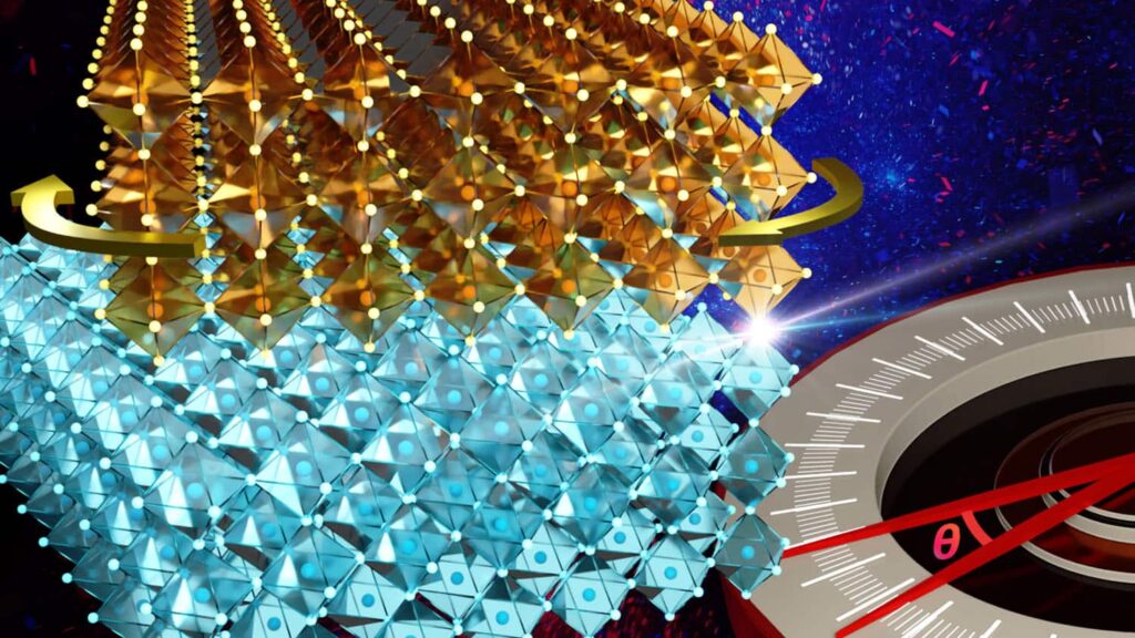
Researchers at North Carolina State University have demonstrated a fabrication technique that produces large-area oxide twistronic materials while maintaining precise control over the twist angles that determine their structural and electronic behaviour. The approach extends twistronics beyond conventional two-dimensional van der Waals materials by using oxide layers that form strong chemical bonds.
The development could help address one of the major limitations in oxide twistronics: fabricating high-quality twisted structures over dimensions suitable for practical devices. According to the researchers, the ability to produce larger crystalline membranes and transfer them onto different substrates offers a route towards scalable twist-engineered electronics for future electronic systems.
To demonstrate the method, the team synthesised crystalline sodium niobate (NaNbO₃) membranes and added photolithographic alignment markers around their edges. One membrane was then lifted and stacked onto another while the markers were used to control the relative twist angle with sub-degree precision, reaching nominal values as low as 0.1 degrees. A material-specific annealing process created strong chemical bonds between the layers, unlike the weak van der Waals interactions commonly used in conventional twistronic materials.
Synchrotron X-ray diffraction revealed that the bonded interface caused gradual rotation of the atomic lattice and altered the material’s phase structure. The researchers also observed changes in ferroelectric domain configurations, indicating that the strong interlayer coupling produces structural reconstruction different from that seen in van der Waals systems. The technique achieved high-crystallinity oxide moiré superlattices across lateral dimensions approaching the millimetre scale and could be adapted to other complex oxide materials beyond sodium niobate.
“Our work demonstrates a technique for creating large-area oxide twistronic materials with controlled twist angles and a strong chemical bond between layers,” says Ruijuan Xu, Assistant Professor of Materials Science and Engineering at North Carolina State University. “It’s an exciting time for oxide twistronics, with new opportunities to engineer complex oxide functionalities through twist.”