
- Sony Corporation’s new image sensors employ SWIR technology for effortlessly capturing images in both visible and invisible light spectrums
- Overcoming the challenges faced by traditional image capturing techniques, the new image sensors help develop cameras and testing equipment for various industrial applications
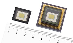 Sony Corporation’s new short-wavelength infrared (SWIR) image sensors for industrial equipment have the capability to capture images in both visible and invisible light spectrum in the short-wavelength infrared range.
Increasing demand to reduce manpower and ensure standardisation in the industrial equipment has led to a growing need for image sensors that can capture images in the invisible light spectrum of the short-wavelength infrared range. However, traditional SWIR image sensors face manufacturing challenges in miniaturising pixels and increasing pixel count, as well as various other issues including low sensitivity in the visible light spectrum and an analogue output that makes multifunctionality difficult. Due to this, there has been an obstruction to penetration.

Seamless image capture
The sensors employ SenSWIR technology, in which photodiodes are formed on an indium gallium arsenide (InGaAs) compound semiconductor layer and are connected via Cu-Cu connection with the silicon (Si) layer which forms the readout circuit — a design which enables high-sensitivity over a broad range of wavelengths.
This approach enables the SWIR image sensor to deliver seamless image capture ability over a broad range of wavelengths – from visible to invisible light spectrum in the short-wavelength infrared range (wavelength: 0.4μm to 1.7μm).
By allowing sensing even in wavelengths not visible to the human eye, it becomes possible to develop cameras and testing equipment for various industrial applications.
The new products also support digital output, matching the performance of current CMOS image sensors for industrial equipment.
Sony plans to implement these products for wider use in a range of industrial applications such as material selection, contaminant inspection and semiconductor inspection.