
- Hamamatsu Photonics presents a liquid-crystal spatial light modulator (SLM) that has a high-pulse laser power capability to achieve precise laser processing
- It is considered to be essential for manufacturing and fabrication techniques of high-strength resistant materials
 Hamamatsu Photonics has developed a liquid-crystal spatial light modulator (SLM) having a high-pulse laser power capability of up to 400 GW/cm2. This new SLM to high-power industrial pulsed laser systems will contribute to achieving high-throughput, high-precision laser processing to processing resistant material such as light-weight and high-strength carbon fibre reinforced plastics (CFRP).
Through this development, innovative manufacturing and fabrication techniques can be carried out by using a cyber-physical system (CPS) that combines cyberspace (virtual space) and physical space (real space) to a highly advanced degree. SLM can freely control the irradiation pattern of a laser.

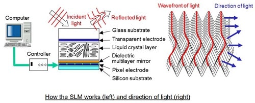
How the SLM operates
A spatial light modulator or SLM is an optical device that utilises liquid crystals to control the wavefront of incident light such as lasers to freely modulate the wavefront shape of the reflected light.
A liquid crystal layer is sandwiched between a silicon substrate with pixel electrodes and a glass substrate with transparent electrodes. The path length of the incident light is varied by controlling the inclination of each liquid crystal according to the signal sent to the pixel electrodes, while the reflected light is modulated for freely controlling the laser irradiation pattern, for example, to branch the incident light or correct its distortion.
Specifications
- Wavelength: 1050 (±50) nm
- Input signal: Digital Video Interface (DVI)
- Input signal level: 256 (8 bits)
- Number of pixels: 1272 × 1024 pixels
- Pixel pitch: 12.5 μm
- Aperture ratio: 95 per cent
- Effective area size: 15.9 × 12.8 mm
What it does
Developed for use with high-power industrial pulsed lasers, the SLM has a high-pulse laser power capability. Lasers are broadly classified into CW (continuous wave) lasers that emit a continuous light beam at constant power and pulsed lasers that repeatedly emit light pulses at short time intervals. Currently, CW lasers are the mainstream of laser machining since they can be used for the heat treatment of metallic materials such as laser welding and cutting.
On the other hand, pulsed lasers can emit light pulses with momentarily high energy allowing high-precision laser machining with minimal heat damage. Because this precision is higher than conventional mechanical machining, pulsed laser machining is becoming widely used for processing resistant materials such as CFRP and low dielectric constant (low-k) materials that prevent a drop in operating speed in semiconductor integrated circuits. However, several issues such as the machining speed and processing throughput remain.
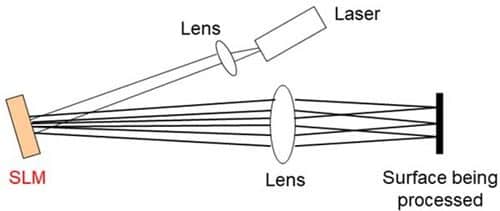
By incorporating an SLM into an industrial pulsed laser system, irradiation of diffracted multiple laser beams is allowed onto different points of target sample simultaneously. This improves the processing throughput compared to laser machining that uses only a single focused beam.
Hamamatsu Photonics’ optical wavefront control devices with high resistance to light are suited for laser marking applications for engraving characters and QR codes on objects moving at high speed on production lines by increasing the light resistance up to 400 GW/cm2 (10 times more than higher than previous products).
Conventional dielectric multilayer mirrors consist of multiple layers made of two types of alternately evaporated material films. At the boundary where these thin films are in contact, the light often interferes with or reinforces other light that can cause damage the thin films. To solve this problem, the thin-films have been designed to suppress the interference of light at the boundaries and minimise adverse effects. The pixel electrode circuit has also been redesigned to suppress unwanted noise.
With this newly developed SLM, a higher power pulsed laser can be used to simultaneously irradiate a target sample with multi-beams while maintaining adequate output power. This helps in achieving high-throughput, high-precision laser processing of processing resistant materials such as CFRP used for aircraft and transportation equipment and low-k materials used for 5th generation mobile communication system (5G).
Future aims
As the device is being viewed essential for new manufacturing and fabrication techniques that utilise artificial intelligence (AI) such as CPS-type laser processing systems, Hamamatsu Photonics is making further improvements to these light resistance properties.
This work has been partially supported by Council for Science, Technology and Innovation (CSTI), Cross-ministerial Strategic Innovation Promotion Program (SIP), “Photonics and Quantum Technology for Society 5.0” (Funding agency: National Institutes for Quantum and Radiological Science and Technology, QST).