




As EV makers shift from silicon to silicon carbide to improve efficiency, reduce costs, and increase power density, new design challenges are emerging. In an interview, Bruno Schuster and Jens Baringhaus from Bosch spoke to Nidhi Agarwal from Electronics For You about the technologies driving the next generation of automotive power semiconductors.

Q: What are the main reasons EV manufacturers are moving from silicon IGBTs to SiC MOSFETs?
Jens: The main reason is higher efficiency. In a battery-powered electric vehicle (EV), replacing silicon insulated gate bipolar transistors (IGBTs) with silicon carbide (SiC) metal-oxide-semiconductor field-effect transistors (MOSFETs) in the traction inverter allows the vehicle to travel farther with the same battery pack or achieve the same driving range with a smaller, lower-cost battery.
Another key advantage is higher power density. Because SiC MOSFETs have lower losses, they enable smaller chips, reduced cooling requirements, and a more compact traction inverter, freeing up space inside the vehicle and supporting greater integration, such as combining multiple power electronic systems into a single unit or enabling compact designs like in-wheel drive systems. In onboard chargers, the primary benefit is also efficiency, ensuring that more of the electrical energy reaches the battery instead of being lost during charging. The higher power density further helps reduce the size of the charger while delivering better performance than conventional silicon-based solutions.
Q: What are the biggest trade-offs engineers face when designing with high-performance SiC devices?
Jens: The biggest trade-off is between performance and robustness. While it is relatively easy to build a high-performance SiC device, making it equally robust and reliable is much more challenging. For Bosch, improving performance at the cost of reliability or robustness is not an option. Every new SiC generation must deliver better performance along with higher reliability and robustness than the previous generation.
Almost every reliability parameter is linked to a performance trade-off, whether it is on-state performance, represented by specific on-resistance, or switching performance. Design choices such as increasing gate oxide thickness or improving the drift region for higher reliability can affect performance. The key is to find the right balance for each application, drawing on Bosch’s experience in automotive systems such as power modules, traction inverters, and onboard chargers.
Q: How do higher switching speeds of SiC devices affect EMI and system design?
Jens: Higher switching speeds in SiC devices introduce additional electromagnetic interference (EMI) challenges. While these can be reduced at the device level by optimising the transistor architecture and accurately measuring EMI during development, they must also be addressed at the system level. Simply replacing a silicon device with a SiC device in an existing design will not deliver the full benefits. To fully utilise SiC’s higher switching speeds and performance, the entire system must be redesigned and optimised, with EMI being one of the key design considerations.
Q: What key trends are shaping the silicon carbide (SiC) ecosystem, from wafer supply to power modules?
Jens: A major milestone for the SiC ecosystem has been the transition to 200mm wafers, while 300mm wafers are already on the horizon. However, for power semiconductor applications, the move to 300mm is not yet commercially justified, and its adoption will depend on the application and the right timing. At the device level, SiC MOSFETs continue to advance through trench architectures with narrower cell pitches and superjunction technology, which promise lower specific on-resistance and higher power density. Although superjunction devices still face challenges, particularly related to the dynamic behaviour of SiC MOSFETs, efforts are underway to address these issues and bring the technology into practical use.
Packaging is another key area of innovation, with embedding technologies emerging as an important trend alongside a growing focus on higher reliability and longer operating lifetimes. This is being driven by demanding applications such as fleet vehicles, robotaxis, and vehicle-to-grid (V2G), vehicle-to-home (V2H), and vehicle-to-load (V2L) systems, where power electronics remain active for much longer periods, often nearly 24/7 instead of only during driving or charging. These evolving requirements are pushing improvements across device technology, packaging, and power module design.
Q: Where do you see the biggest opportunities for standardisation in the SiC ecosystem?
Jens: The strongest case for standardisation is in the power module segment, where common footprints, cooling solutions, and mechanical dimensions can reduce costs, simplify integration, and increase production volumes through economies of scale. For power semiconductor chips, however, standardisation should be limited to areas such as reliability testing, measurement methods, and characterisation, while leaving device architectures open to competition. Different chip designs continue to drive rapid improvements in power density, efficiency, performance, and ultimately cost, so standardising internal architectures could slow innovation.
From the customer perspective, the market includes both high-performance users, who value differentiated technologies, and commodity-focused customers, who prefer standardised, interchangeable components at the module level and sometimes even at the die level. Suppliers therefore need to balance both needs by offering standard products alongside differentiated solutions. Standardising external interfaces, such as die size, layouts, bond pad locations, gate pad positions, footprints, and module dimensions, can improve compatibility, but the internal chip architecture should remain flexible because preserving design innovation is essential for continued advances in performance, reliability, and cost reduction.
Q: What drove Bosch to develop the third generation of silicon carbide technology for EV powertrains?
Jens: The objective was to build on the capabilities of earlier silicon carbide generations by increasing power density and current density. Higher power density enables the same power output with a smaller chip, reducing the amount of silicon carbide needed. This lowers the cost of the device while also allowing more compact power electronics. Although silicon carbide delivers higher efficiency than conventional silicon, its higher cost has limited its adoption in many applications. By reducing chip size and cost, the third-generation technology makes silicon carbide more affordable for cost-sensitive EV applications, supporting its use across a wider range of vehicles.
Q: What were the key design challenges in developing your third-generation silicon carbide devices, and how did you address them?
Jens: One of the biggest challenges in designing silicon carbide devices is balancing performance and robustness. Lower specific on-resistance improves power density by allowing the chip to be smaller while handling higher power, but the device must also remain reliable during off-state operation, when high electric fields can stress the gate structure. In our third-generation silicon carbide devices, we addressed this challenge by retaining our proven trench technology and introducing a new shielding design element to better protect the gate.
This new shielding structure enabled us to reduce specific on-resistance and increase power density while also improving off-state robustness. The devices offer better resistance to cosmic radiation, improved gate oxide reliability and lifetime, and higher short-circuit withstand capability, which is especially important for traction inverter applications. Instead of making a trade-off between performance and robustness, our third-generation design improves both at the same time.
Q: What role did simulation play in optimising the architecture of Bosch’s Generation 3 silicon carbide chips?
Jens: Simulation is one of the core pillars of semiconductor and power semiconductor development, alongside process development. It is used to define new device generations, develop manufacturing processes, evaluate process tolerances early, and predict device performance under real-world operating conditions through both static and dynamic simulations.
For Generation 3, simulation played a key role from the concept stage. We carefully calibrated the simulation models to accurately represent both the device architecture and the manufacturing processes. In addition to simulating the devices, we also model production processes to understand how process changes and variations affect device performance, allowing us to optimise both the design and manufacturing process before production.
Q: Which qualification tests were most critical before releasing the Generation 3 chips?
Jens: Our Generation 3 chips are built on the same well-established technology platform introduced with Generation 1, which was already qualified to meet all relevant automotive standards. However, from the beginning, we have gone beyond standard automotive qualification requirements such as AEC-Q101. We use longer test durations and more demanding stress conditions to ensure higher reliability.
We followed the same approach for Generation 3. In fact, there were no additional qualification challenges because the new generation was designed for even greater robustness. Lifetime testing shows that Generation 3 devices can support longer operating lifetimes and more demanding mission profiles. They can withstand higher drain voltages, including future 1000V battery systems, as well as higher gate voltages and voltage overshoots.
Q: Besides the new shielding architecture, what other changes have been introduced in this new generation of chips?
Jens: The biggest innovation is the redesigned shielding region. We have retained the proven cell architecture from our second-generation devices but added a new shielding element to better protect the gate trench. This shielding region is manufactured using a self-aligned process, which ensures it is perfectly aligned with the gate trench. This is important because the gate trench contains the gate oxide, one of the most sensitive parts of a power transistor. Precise alignment ensures the shielding performs exactly as intended, improving the device’s reliability and robustness.
Apart from the shielding improvement, we have also reduced the chip thickness. While our first- and second-generation chips were 180 microns thick, the third generation was only 100 microns thick. This brings two key benefits. First, the lower substrate resistance helps reduce the on-resistance of the device, improving efficiency. Second, the thinner chip improves thermal performance by reducing thermal resistance, allowing heat to dissipate more effectively.
Q: The new generation claims around a 20 per cent performance improvement. Which device parameters contribute most to this gain?
Jens: The 20 per cent improvement mainly comes from better on-state performance, specifically lower on-resistance, which helps the device conduct current more efficiently. This is achieved through improvements in the transistor cell architecture, especially the redesigned shielding region. The new shielding lowers resistance during normal operation while maintaining strong short-circuit withstand capability. This helps overcome the traditional trade-off between low on-resistance and robustness under high drain voltages.
The improved shielding architecture also enhances the device’s dynamic performance. It reduces gate-drain capacitance and gate-drain charge, enabling faster switching and lower switching losses. In addition, the intrinsic body diode performance has been improved, further supporting faster switching. Depending on the application, module design, and package, switching losses can be reduced by around 10 to 15 per cent when moving from the second-generation to the third-generation device.
Q. How is your Generation 3 SiC technology technically different from competing solutions in the market?
Jens: Generation 3 was developed using extensive feedback from both Bosch’s internal power electronics teams and external customers to make it the best fit for automotive applications. A major focus was optimising the balance between performance and robustness, as power semiconductor design involves many trade-offs. A device that delivers very high performance but compromises reliability can lead to field failures and customer dissatisfaction. Rather than maximising a single parameter, Bosch focused on identifying the optimum point across these trade-offs to ensure both strong performance and long-term reliability.
Another key differentiator is Bosch’s in-house automotive system expertise. The company can directly apply knowledge gained from developing complete automotive power electronic systems to its chip design, allowing devices to be optimised for real-world application requirements instead of only chip-level performance. According to Bosch, this depth of system knowledge is not typically available to companies that focus only on silicon carbide chips, modules, or semiconductor supply, giving Bosch an advantage in developing automotive-focused SiC technology.
Q. What engineering innovations have made miniaturisation possible?
Jens: Increasing the number of chips per wafer is driven by two factors. First, reducing the specific on-resistance increases power density, allowing smaller chips to deliver the same performance, which means more dies can fit on a wafer. Second, Bosch has significantly improved manufacturing yield. Unlike silicon, silicon carbide naturally contains many crystal defects, making completely defect-free devices impossible. Bosch invested heavily in understanding how different defect types, their density, and their location within the device affect electrical performance and, more importantly, long-term reliability. This enabled the company to define acceptable defect thresholds and the substrate quality needed to meet its reliability targets.
These improvements have steadily increased the number of usable dies per wafer while also making it possible to manufacture much larger devices. For example, Generation 3 introduces an 80mm² die, which would not have been commercially viable a few years ago because yields were too low. Higher yield and better quality now allow Bosch to offer a broader range of die sizes, giving customers the flexibility to choose either a few larger dies or multiple smaller dies depending on their application and preferred level of parallelisation.
Q: What barriers still limit wider silicon carbide adoption in cost-sensitive EV platforms, and how does Generation 3 address them?
Jens: Cost remains one of the main barriers for wider silicon carbide adoption, especially in cost-sensitive EV platforms. Generation 3 addresses this by reducing the required die size, which lowers the overall device cost. In addition, Bosch is introducing variants of Generation 3 with slightly reduced robustness targets. These variants still maintain the same robustness level as Generation 2 while offering better performance and allowing even smaller die sizes than the standard Generation 3 devices. They are particularly suited for applications with lower battery voltages and lower voltage requirements, such as 400V battery systems, where cost sensitivity is higher. This makes silicon carbide a more affordable choice for a wider range of vehicle platforms.
Q: How much improvement can original equipment manufacturers (OEMs) expect in vehicle efficiency and range with Generation 3 silicon carbide devices?
Jens: The biggest benefit of Generation 3 is cost reduction rather than a major increase in vehicle range. The smaller die size helps lower the cost of silicon carbide devices, making them more accessible for more EV platforms. In terms of efficiency, Generation 3 delivers a 10 to 15 per cent reduction in switching losses. Since switching losses account for a large share of traction inverter losses during partial-load operation—where EVs operate most of the time—this directly improves inverter efficiency. However, the largest efficiency gain comes from replacing conventional silicon devices with silicon carbide. Generation 3 makes that transition more affordable, particularly for cost-sensitive 400V EV platforms, allowing silicon carbide to be used across a wider range of applications while delivering both better efficiency and lower system cost.
Q: How does Bosch ensure consistent silicon carbide device performance across wafers, and what investments is it making to support high-volume production?
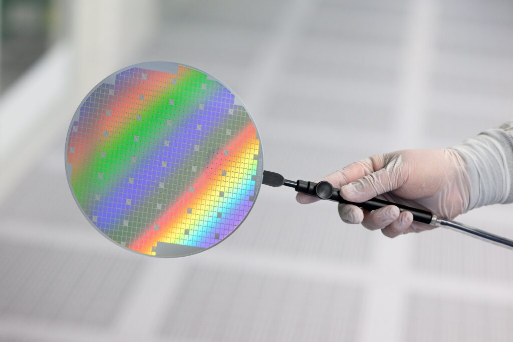
Jens: Our transition from 150mm to 200mm wafer manufacturing has been a major step. As of this year, both our Reutlingen, Germany, and Roseville, California fabs manufacture silicon carbide devices exclusively on 200mm wafers. These fabs are highly automated, with automated wafer loading, scheduling, and processing, which reduces particle contamination and ensures every wafer is processed consistently. The move to 200mm also enables the use of more advanced processing equipment, improving wafer-to-wafer consistency and on-wafer parameter uniformity.
To support high-volume production, we have expanded 200mm processing capacity at our Reutlingen site and established a second 200mm silicon carbide fab in Roseville, California. Both fabs use the same production processes, equipment, and recipe sets, ensuring consistent product quality while providing a stable supply from two geographically independent manufacturing locations and enabling reliable deliveries to customers.
Q: What packaging innovations were introduced alongside your latest silicon carbide die?
Jens: Alongside the new silicon carbide die, we also advanced our packaging technologies for both power modules and discrete devices. For power modules, we developed an extremely low-inductance package so that the fast-switching capability of the silicon carbide die is not limited by the package itself. For discrete devices, we focused on more compact packages with reduced height and a smaller footprint, allowing either a smaller silicon carbide footprint or more die area to fit into the same package, which helps improve power density.
Another key focus was thermal performance. Silicon carbide devices can operate at higher continuous junction temperatures to increase power density, but the package and module architecture must also support these higher temperatures. Packaging innovations therefore play a critical role in ensuring that the benefits of the silicon carbide die can be fully realised.
Q: What packaging challenges remain for high-power automotive silicon carbide devices?
Jens: The biggest challenges are continuing to increase power density, reduce inductance, handle higher operating temperatures, and improve interconnection reliability. These are not packaging-only challenges—they require close co-design between the chip and the package. For example, embedding power devices into a printed circuit board (PCB) can deliver extremely high power density and very low-inductance modules, but this requires the chip to support copper power metallisation, a feature included in our third-generation silicon carbide devices. The same metallisation also enables direct copper wire bonding without an aluminium layer, creating an all-copper interconnection stack that offers excellent power-cycling reliability.
Thermal management is another major challenge. As chip sizes shrink while power density increases, more heat is generated in a smaller area. Packaging technologies and cooling techniques must therefore continue to evolve to efficiently remove heat from these localised hotspots while keeping pace with the higher junction temperatures enabled by silicon carbide devices.
Q: How important is local ecosystem development for accelerating silicon carbide adoption in India?
Bruno: A strong local ecosystem is essential for accelerating silicon carbide adoption, but it is still developing in India. While the electrification ecosystem is taking shape, the silicon carbide ecosystem is yet to mature. In regions like China, local development teams, application engineering, product management, and customer support have been key to driving adoption. In India, we are building a one-stop offering that covers complete drivetrain systems, inverters, modules, and bare dies. We have also formed a joint venture with Tata AutoComp Systems to offer complete e-Axles integrating electric motors, inverters, and transmission units.
Q: What trends are you seeing among Indian EV manufacturers regarding silicon carbide adoption?
Bruno: Indian EV manufacturers are not asking for something fundamentally different from global customers, but the market is at an earlier stage of adoption. Most EVs currently use 400V battery systems and remain highly cost-driven, with IGBT technology widely used. Silicon carbide adoption is only beginning, and local availability is still limited, with most solutions coming from international suppliers. As electrification expands and higher-voltage platforms become more common, we expect silicon carbide adoption in India to grow steadily over the next five years, following the trend seen in other regions.
Q: Which vehicle segments in India are likely to adopt silicon carbide (SiC) first?
Bruno: SiC is typically used in 800V electric vehicle platforms, particularly in premium and high-performance vehicles that support features such as fast charging. We expect adoption to begin in these segments and gradually expand to smaller vehicles because the benefits of higher efficiency, better performance and battery savings apply across all vehicle categories. Our third-generation SiC technology is suitable for everything from heavy-duty and medium-duty commercial vehicles to passenger cars, including small A-segment vehicles. It can also be used in India’s large two-wheeler market, although that segment is not yet ready for SiC adoption.
Q: Is Bosch working with Indian OEMs or Tier-1 suppliers on SiC-based powertrain development?
Bruno: Bosch already works with Tata through its electrification joint venture on electric motors and complete drivetrain systems. However, we do not currently have silicon carbide-specific partnerships in India, as the market is still at a very early stage. We are in discussions with various OEMs and closely tracking when the market is ready. Bosch is prepared to support India with its SiC solutions and has a dedicated mobility team that adapts global innovations to local market requirements.
Q: Does Bosch plan to expand SiC-related R&D, engineering, or manufacturing activities in India?
Bruno: At present, support for the Indian market comes from our headquarters in Germany and our Asia-Pacific headquarters in Shanghai. As the market grows, we plan to establish local teams for development, application engineering, and project management. Having local expertise is important for serving customers more effectively and responding faster to market needs. We are ready to begin that journey as SiC adoption in India increases.
Q: What technologies are shaping Bosch’s next generations of silicon carbide devices, and what can we expect from the fourth and fifth generations?
Bruno: We develop multiple silicon carbide generations in parallel rather than sequentially, allowing us to accelerate innovation. Our fourth-generation devices, which entered development several years ago, are planned for launch in about two years, while the fifth generation is already in pre-development for launch roughly four years from now. The key focus is further improving power density. Generation 4 will reduce the cell pitch by half, enabling higher power density, and its cell architecture will also form the basis of Generation 5. The fifth generation will combine this architecture with superjunction technology, using a superjunction drift zone to significantly reduce drift-zone resistance and further increase power density.
Beyond new device architectures, we are improving every part of the device, including the substrate, die thickness, gate oxide, gate stack, and manufacturing processes. Process innovations are especially important as we move to superjunction technology because they help reduce manufacturing costs while maintaining performance. By advancing device architecture and process technology together and by developing multiple generations simultaneously, we can deliver new technologies much faster than would be possible with a generation-by-generation development approach.
Q: How do you see silicon carbide evolving alongside GaN (gallium nitride) in automotive power electronics?
Bruno: We are actively developing gallium nitride technology within Bosch while also evaluating existing GaN solutions for applications such as traction inverters and onboard chargers. Based on our assessment, silicon carbide currently offers the best overall cost-performance for most automotive applications. In traction inverters, where high power density, compact device size, and excellent thermal performance are critical, silicon carbide clearly outperforms gallium nitride. This is particularly true for 800V and higher battery systems, although silicon carbide also remains difficult to beat at lower battery voltages with the GaN solutions currently available. For onboard chargers, gallium nitride benefits from lower switching losses and better dynamic characteristics because of its higher switching frequencies, but when the entire system is considered, silicon carbide often remains the more cost-effective solution. GaN is promising, but SiC still sets the benchmark for automotive power electronics.
Gallium nitride continues to evolve with innovations such as bidirectional switches for single-stage onboard chargers, which could become disruptive. However, we have also introduced our first silicon carbide bidirectional switch in a standard Q-DPAK package, offering similar functionality with strong cost-performance advantages. Overall, we believe silicon carbide currently has an edge across most automotive applications, while gallium nitride still needs to prove that it can consistently meet automotive requirements for reliability, lifetime, and robustness, particularly in areas such as short-circuit capability, where silicon carbide has already demonstrated strong performance.
Q: What should power electronics engineers focus on today to prepare for the next generation of automotive power semiconductors?
Bruno: Engineers should keep an open mind and be ready to adapt their system designs to make the best use of new power semiconductor technologies. Power semiconductor companies continue to introduce innovations that improve device performance, but many of these benefits cannot be fully realised unless the overall system is designed to support them.
For example, next-generation devices switch much faster and offer much higher power density, which requires better system design, advanced cooling solutions, and improved thermal management. Innovation, therefore, has to happen at both the semiconductor and system levels. When the pace of innovation in devices and system design stays aligned, power electronics can deliver its full potential in automotive applications.


