
In the world of semiconductors and microelectronics, a trend to vertically stack integrated circuits (ICs) or circuitry has emerged as a viable solution for meeting electronic device requirements such as higher performance, increased functionality, lower power consumption, and a smaller footprint. The various methods and processes used to achieve this are called 3D integration technologies.
Overview
Next-generation platforms are evolving rapidly to keep pace with emerging system trends driven by an explosion of applications such as data center capabilities, Internet of Things (IoT), 400G to terabit networking, optical transport, 5G wireless, 8K video, etc. The resulting expansion of connectivity and processing will affect the semiconductor space significantly, from the type of components that are built to higher efficiency systems and related services.
A close evaluation of this emerging landscape reveals some interesting trends. For example, next-generation data center workloads demand increasingly higher computational capabilities, flexibility, and power efficiencies; outstripping the capabilities of today’s general-purpose servers. Additionally, data center infrastructure must be virtualized and delivered as a service over commodity servers to reduce complexity and provide greater business agility and scalability. However, server performance improvements have actually slowed, primarily due to power limitations. Designing data center solutions for specific workloads increases efficiency but significantly limits the homogeneity and flexibility of the solution. Flexibility is crucial because data center services evolve rapidly and require adaptable hardware. As a result, the challenge for next-generation data center platforms is to deliver higher performance (acceleration), power efficiency, and flexibility simultaneously.
IoT reflects similar challenges. IoT is projected to grow dramatically and hit the multibillion “smart objects” mark in the near future. These smart objects are connected and communicate with each other or to a cloud or data center. The infrastructure must determine which data needs to be processed and which data is dropped, all in real time. Therefore, IoT requires a highly connected, flexible, efficient, bandwidth-rich infrastructure that enables insight from the data center to the edge. This requirement challenges service providers, data centers, cloud computing, and storage systems to satisfy this insatiable demand for Internet traffic.

Thus, system architects designing next-generation platforms must try to meet the following requirements:
■ Higher bandwidth
■ Lower power
■ Smaller footprint or form factor
■ Increased functionality
■ Increased flexibility
3D integration technology has become the most widely used technology to achieve the above said requirements.
What is 3D Integration?
There are certainly different understandings in the microelectronics community regarding the definition of heterogenous 3D integration. In a very general definition, it is defined as the 3D integration of different devices such as a CMOS processor and a memory, for example. A more limiting specification would define it as the integration of different substrate materials necessary for the condition (e.g. GaAs / silicon). For the purpose of this article, we will define it as the 3D integration of components with significant different device technologies as e.g. CMOS and MEMS.
Scope in Industry
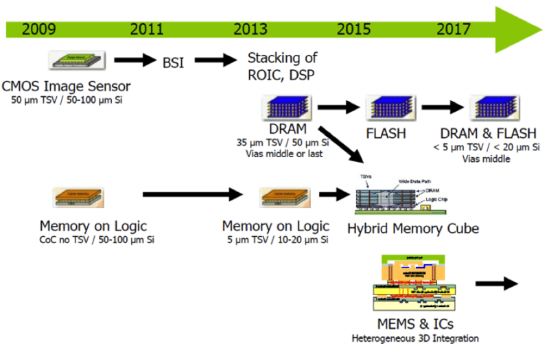
3D integration is now considered to be a new paradigm for the semiconductor industry. There are various ways to vertically interconnect devices, with most advanced technology based on through-silicon vias (TSV). As expected, IBM, Samsung, Micron, TSMC, Hynix and STATS ChipPAC are the leading players concerning the number of patents held. On the other hand, relevant patents on 3D integration are also found among different academic institutions with ITRI being the top institute, followed by CEA (France) and Fraunhofer-Gesellschaft München (Germany). Apparently Europe is strong in intellectual properties for 3D ICs. World-wide, memory-enhanced applications are seen as the main driver for 3D Integration. With the maturity of heterogeneous 3D integration technologies and corresponding low-cost fabrication, a diversity of 3D integrated CMOS-MEMS products will be developed, leading to a further key application track .
3D System-In-Package Technology
Heterogeneous 3D SiP technology allows various components to be integrated alongside an FPGA into a single package to match system requirements, effectively providing robust solutions more quickly than in previous generations. This approach enables in-package integration of a range of components such as analogue, memory, ASIC, CPU, etc
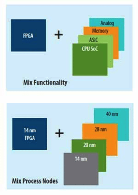
The approach to heterogeneous 3D SiP integration is unique in the FPGA industry in that it uses a single monolithic FPGA core fabric (up to 5.5 million logic elements) and integrates multiple die around the FPGA. A monolithic FPGA core fabric provides maximum performance and utilization, and ensures that data can be processed at the highest rates possible without running into routing congestion, utilization bottlenecks, or degraded performance.
The technology that makes broad deployment possible is Intel’s patented, Embedded Multi-die Interconnect Bridge (EMIB). Intel designed EMIB for solutions that require advanced packaging and test capabilities. EMIB provides a simple integration flow and offers an ultra-high-density interconnect between heterogeneous die in the same package. It also enables in-package functionality that was either too complex or too cost prohibitive to implement with alternative in-package integration solutions.
These new class of products will meet the system functionality requirements of today and those of the future, including:
• Higher Performance / Bandwidth
System-In-Package integration using EMIB, enables the highest interconnect density between FPGA and the companion die. This results in high bandwidth connectivity between the SiP components. In addition, user signals communicating to external world use standard FCBGA traces, thereby improving signal and power integrity.
• Lower Power
Companion die (such as memory etc) are placed as close as possible to FPGA. The interconnect traces between the FPGA and the companion die are thus very short and don’t need as much power to drive them. This results in lower power overall and the most optimum performance/watt metric.
• Smaller Form Factor
The ability to heterogeneously integrate components in a single package results in smaller form factors. This helps customers save valuable board space, reduce board layers and overall build of material (BOM) cost.
• Greater Flexibility, Scalability and Ease of Use
SiP helps reduce routing complexity at the PCB level since the components are already integrated within the package. In addition, SiP enhances the ability to incorporate different die geometries, silicon technologies. Net result is a highly flexible, scalable solution that is easy to use.
• Faster Time to Market
SiP enables faster time to market by being able to integrate already proven technology and reuse common devices or tiles across product variants. This saves valuable time and resources, thereby helping customers accelerate their time to market.
Conclusion
Next-generation platforms increasingly require innovative solutions that provide significantly higher performance, lower power, and smaller form factors. The explosion in data center capabilities and proliferation of IoT technologies are emerging as key drivers. In addition, advancements in terabit networking, optical transport, 8K video, and 5G wireless domains are ramping up rapidly, forcing the semiconductor ecosystem to find innovative solutions.
He is currently pursuing B.Tech in ECE from RSET, Cochin