


A Binary Adder is a digital circuit that performs the arithmetic binary addition of two numbers for the logic operations and laws of Boolean Algebra.
The adders are used in combinational circuit design and the microprocessor’s arithmetic logic unit (ALU) for calculating addresses.

There are two types of Adder Circuits in Digital Electronics–
- Half Adders
- Full Adders
Table of Contents
Half Adder
Half Adder is a digital circuit to calculate the arithmetic binary addition of two single-bit numbers. It is a circuit with two inputs and two outputs.
For two single-bit binary numbers A and B, half adder produces two single-bit binary outputs S and C, where S is the Sum and C is the carry.
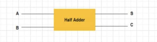
The sum is for the least significant bit (LSB) and carry is for the most significant bit (MSB).
Operation and Truth Table for Half Adder
Operation:
Case 1: A= 0, B= 0;
According to Binary addition, the sum of these numbers is 0 with no carry bit generation.
0
+ 0
一一一一一
0
一一一一一
Hence, S= 0, C= 0
Case 2: A= 0, B= 1;
As per Binary addition, the sum of these numbers is 1 with no carry bit generation.
0
+ 1
一一一一一
1
一一一一一
Hence, S= 1, C= 0
Case 3: A= 1, B= 0;
As per Binary addition, the sum of these numbers is 1 with no carry bit generation.
1
+ 0
一一一一一
1
一一一一一
Hence, S= 1, C= 0
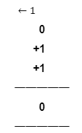
Case 4: A= 1, B= 1;
According to Binary addition, the sum of these numbers is 1 with a carry bit generation of 1.
1
1
+ 1
一一一一一
0
一一一一一
Hence, S= 0, C= 1
Half Adder Truth Table:
| A | B | Sum (S) | Carry (C) |
| 0 | 0 | 0 | 0 |
| 0 | 1 | 1 | 0 |
| 1 | 0 | 1 | 0 |
| 1 | 1 | 0 | 1 |
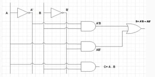
Designing Half Adder
With the help of the Truth Table, We can design a Karnaugh Map or K-Map for Half Adder to obtain a Boolean Expression.
Karnaugh Map for Sum:
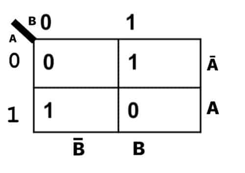
By solving this,
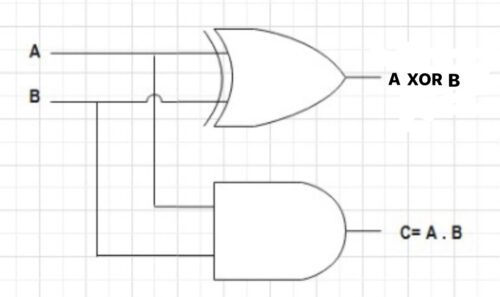
S= A’B + AB’

Karnaugh Map for Carry:
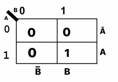
By looking at the K-map, We can conclude;

This Boolean expression helps us to design a half adder with an XOR Gate and AND gate.
The operation of Half Adder is limited because it can only add two-bit binary digits. But in practical applications, we need to add three or more bits.
This inability of the circuit puts a limitation on its use. Half-adders were used in early microprocessors and basic digital circuits.
Designing Half Adder using Basic Gates followed by NAND Gate
As
S= A’B + AB’
Taking double complement
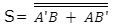
According to d-Morgan’s law,

Note: Using NAND Gate only
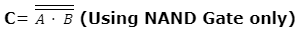
Similarly, for the carry circuit,
C= A.B
Taking double complement
Full Adder
Full Adder is a digital circuit that adds three single-digit binary numbers. This is a three-input and two-output digital circuit.
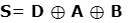
For three single-bit binary numbers A, B, and D; the full adder circuit generates two single-bit binary outputs S (Sum), and C (Carry).

Full Adder was made to overcome the limitations of Half Adder.
Full Adders Uses
- Digital Diaries
- Digital Calculator
- Digital Computer
- Arithmetic Logic Unit (ALU) of Microprocessors.
Operation and Truth Table for Full Adder
Operation:
Case 1: A= 0, B= 0, and D= 0;
The sum of the three binary numbers 0, 0, and 0 yields a sum of 0 and generates no carry bit.
0
+0
+0
一一一一一
0
一一一一一
Hence, S= 0, C= 0
Case 2: A= 0, B= 0 and D= 1;
The sum of the three binary numbers 0, 0, and 1 yields a sum of 1 and generates no carry bit.
0
+0
+1
一一一一一
1
一一一一一
Hence, S= 1, C= 0
Case 3: A= 0, B= 1, and D= 0;
The sum of the three binary numbers 0, 1, and 0 yields a sum of 1 and generates no carry bit.
0
+1
+0
一一一一一
1
一一一一一
Hence, S= 1, C= 0
Case 4: A= 0, B= 1 and D= 1;
The sum of the three binary numbers 0, 1, and 1 generates a carry bit 1.
This makes the sum to be 0.
Hence, S= 0, C= 1
Case 5: A= 1, B= 0 and D= 0;
The sum of the three binary numbers 1, 0, and 0 yields a sum of 1 and generates no carry bit.
1
+0
+0
一一一一一
1
一一一一一
Hence, S= 1, C= 0
Case 6: A= 1, B= 0 and D= 1;
The sum of the three binary numbers 1, 0, and 1 generates a carry bit 1.
This makes the sum to be 0.

1
+0
+1
一一一一一
0
一一一一一
Hence, S= 0, C= 1
Case 7: A= 1, B= 1 and D= 0;
The sum of the three binary numbers 1, 1, and 0 generates a carry bit 1.
This makes the sum to be 0.
1
+1
+0
一一一一一
0
一一一一一
Hence, S= 0, C= 1
Case 8: A= 1, B= 1 and D= 1;
The sum of the three binary numbers 1, 1, and 1 generates a carry bit 1.
The sum of the first 1 and 1 is 0 with a carry bit 1.
The sum 0 gets added to the third bit 1 and the carry gets further to MSB.
This makes the sum 1.
1
+1
+1
一一一一一
1
一一一一一
Hence, S= 1, C= 1
Full Adder Truth Table:
| A | B | D | S (Sum) | Carry (C) |
| 0 | 0 | 0 | 0 | 0 |
| 0 | 0 | 1 | 1 | 0 |
| 0 | 1 | 0 | 1 | 0 |
| 0 | 1 | 1 | 0 | 1 |
| 1 | 0 | 0 | 1 | 0 |
| 1 | 0 | 1 | 0 | 1 |
| 1 | 1 | 0 | 0 | 1 |
| 1 | 1 | 1 | 1 | 1 |
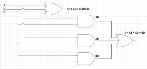
Designing Full Adder
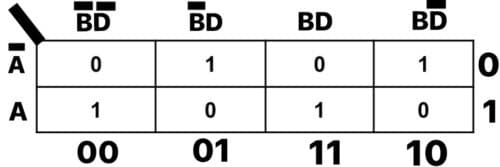
With the help of the Truth Table, We can design a Karnaugh Map or K-Map for Full Adder to obtain a Boolean Expression.
Karnaugh Map for Sum of Full Adder:
By Solving this,
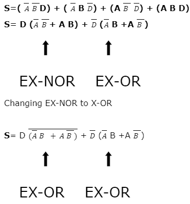
The terms ![]() and
and ![]() form a complement of each other, the whole equation becomes an EX-OR operation;
form a complement of each other, the whole equation becomes an EX-OR operation;
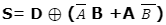
Simplifying further,
Karnaugh Map for Carry:
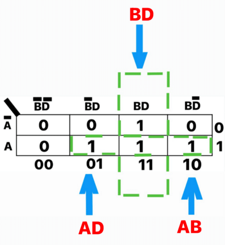
The equation becomes,
C= AB + AD + BD
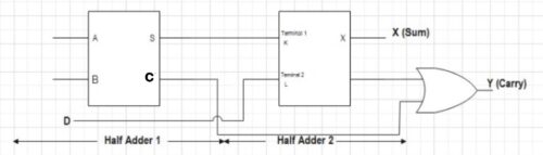
Designing Full Adder using two Half adders
Construction:
The inputs of the first half adder are two single binary digits A and B. The output of the first half adder sum S is fed to the input of the second half adder terminal 1 on K. The sum output of the second half adder is obtained across X.
The carry bit D is directly applied across terminal 2 on L of the second half adder. The carry output is obtained across Y of the second half adder.
Operation:
The Boolean expression for Output Sum at S of the first half adder

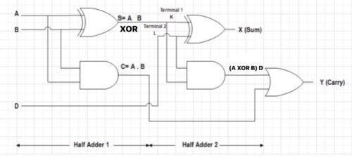
The output across the second half adder for Sum X is a direct EXOR operation of S of the first half adder at input terminal 1 and the carry bit at input terminal 2 of the second half adder
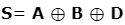
Hence, the expression for the sum of two half adders is the same as the sum of the Full Adder circuit.
The Boolean expression for Output Carry at Y is an OR operation of the output carry of both the first and second-half adders.
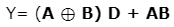
For this, we have to solve the Boolean expression.
By circuit diagram,
Y= (A’B + AB’) D + AB
Y= A’BD + AB’D + AB
By inserting the Boolean Law of OR,
1+D= D
Y= A’BD+ AB’D + AB (1+D)
Y= A’BD+ AB’D + AB + ABD
Y= BD (A’+A) + AB’D + AB
By using the Boolean Law of OR,
A+A’= 1
Y= BD + AB’D + AB
By inserting the Boolean Law of OR,
1+D= 1
Y= BD + AB’D + AB (1+D)
Y= BD + AB’D + AB + ABD
Y= BD + AD (B’+B) + AB
By using the Boolean Law of OR,
B+B’= 1
Y= BD + AD + AB
The expression for Carry of two half adders is the same as that of a Full Adder.
Hence, when two half-adders are connected, they behave as full adders and perform all the operations of a full adder.
We hope now you have a clear idea about Half Adder and Full Adder; Still, if you have any doubts, feel free to ask in the comments below.
Also Read: