


The nanometer (nm) process world is a great mess. Today we see 350nm to 90nm in declining mode, 65nm to 32nm still moving towards maturity and 22nm to 14nm in growth mode. If we extrapolate this trend to 7nm and then 5nm and 3nm beyond 2020, we can envision that, by that time 14nm and 10nm will be in major production. Fin field effect transistor (FinFET) process will be perfected with 16nm, 14nm and 10nm, which will be adopting the same technology with improved performance.
Single-transistor 7nm-scale devices were first produced in early 2000s; commercial production of 7nm chips is still at a development stage. Most semiconductor production equipment being used for fabrication of 10nm chips are used for 7nm manufacturing. 7nm chips are 10 to 15 per cent faster than 10nm chips, while reducing power consumption by 35 to 40 per cent.

A nanometre is a billionth of a metre. In the next six years, manufacturers plan to make chips with features measuring from 100nm to 70nm, using deep ultraviolet light of 193nm and 157nm wavelengths. Silicon has already managed to fabricate FinFET transistors using InGaAs and InP on a 300mm 22nm silicon wafer a year and a half ago.
Thanks to the silicon-germanium process, we may soon witness the first functional transistors with 7nm technology. The fundamental flaw with silicon transistors is that, at 7nm point the transistors sit so close to each other that an effect called quantum tunneling occurs. This effect unfortunately means that the transistor cannot be turned off reliably and for the most part will stay on. So the physical limitations of silicon are very real and, in fact, insurmountable.
One alternative is to find a material that can physically scale down past silicon or can achieve faster switching speeds. The other is to rely on something other than electricity to achieve/read on or off states, such as light. However, there is one very promising short-term silicon alternative that will most likely supersede silicon in a few years.

III-V semiconductors, which were originally expected to debut at 10nm, are now being pushed back to 7nm or 5nm due to ongoing manufacturing difficulties. Chips suffered from lengthy delays due to tick-tock manufacturing schedules. Foundries have managed to create the world’s first working version of a 7nm chip, which promises to be twice as dense as next-generation 10nm chips, and even denser than today’s 14nm chips. This breakthrough should enable the building of chips that have more than 20 billion transistors. Creation of the working samples of chips with 7nm transistors is achieved by moving away from pure silicon to silicon-germanium alloy for making the transistors.
The new material has higher electron mobility and makes it possible to have faster switching transistors and lower power requirements. Light is directed onto a mask, which is sort of a stencil of an integrated circuit pattern. Image of that pattern is then projected onto a semiconductor wafer covered with light-sensitive photo-resist. Creating circuits with smaller and smaller features requires shorter and shorter wavelengths of light.
Technology node
In semiconductor manufacturing, we define the 7nm node as the technology node following the 10nm node. Node is merely a label for a group of technologies that deliver an improvement rather than a measure of half-pitch or gate length. The term node is used by the semiconductor industry to characterise major targets in their manufacturing roadmap.
Transistors involve fin-shaped pieces of silicon, where each fin is about 14nm wide, 60nm to 70nm tall and 100nm or longer.
 Gate-all-around FETs are the most likely approach at 7nm, with germanium as a channel option, which assumes that certain difficulties of adapting germanium for n-channel can be overcome. Currently, germanium is an excellent p-channel material but more difficult to work with for n-channel. Slow caches can recognise substantial gains over 28nm, but fast cache scarcely improves over the current generation. If gate-all-around and other technologies get perfected by, say, 2025, these may take over by 2030.
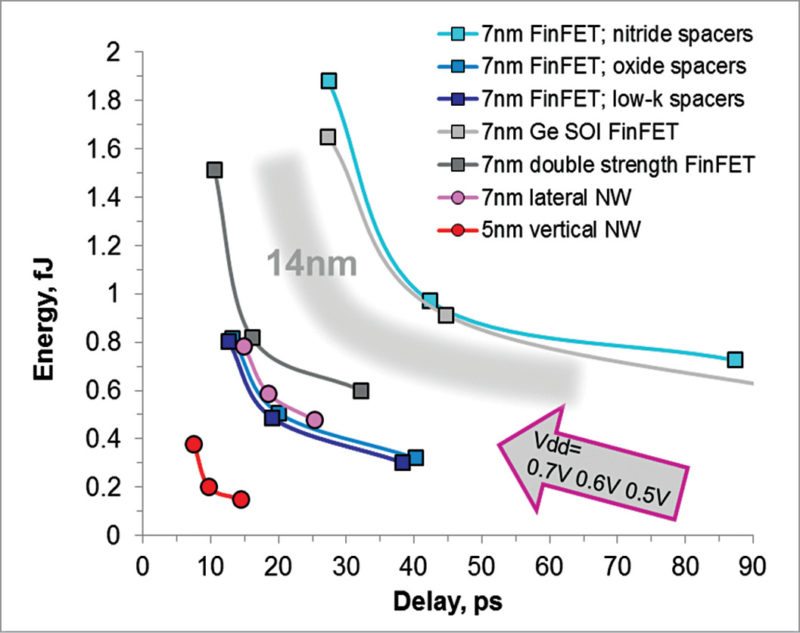
In any case, there are two basic transistor candidates at 7nm: FinFET and lateral gate-all-around nanowire FET, sometimes called lateral nanowire FET. At 5nm, the industry is leaning towards lateral nanowire FET. For 7nm FinFETs, chipmakers need to make the fins taller to boost drive current. FinFETs also have new channel materials to boost mobility.
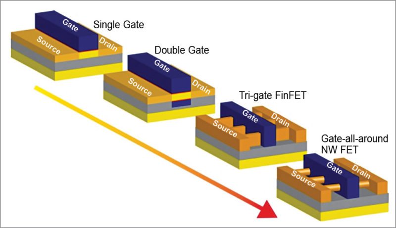
The second option, lateral nanowire FET, is basically an evolutionary step from FinFET. It increases the gate area, so that you are more effective at turning off the device.
Nanowire FETs provide better electrostatics than FinFETs, but nanowire FET is more difficult to make in a fab. Still, FinFET and nanowire FET use many of the same process steps. One of the main differences is that nanowire FETs require complex processes on the bottom of the device. For 5nm, or even for 7nm, foundry experts are gearing up to develop further next-generation transistors; front runner among these seems to be what is called gate-all-around transistor.Gate-all-around FETs are similar in concept to FinFETs, except that gate material surrounds the channel region on all sides. Depending on design, gate-all-around FETs can have two or four effective gates.
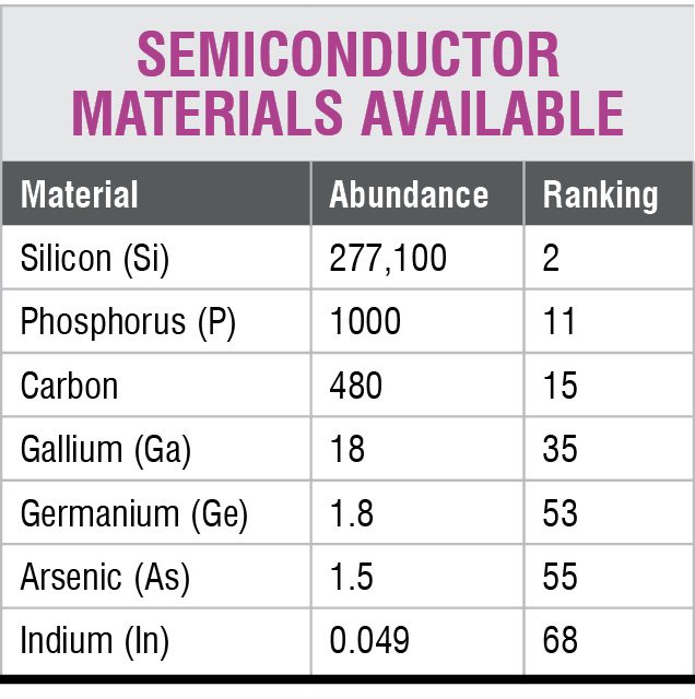
Gate-all-around FETs have been successfully characterised both theoretically and experimentally. These have also been successfully etched onto indium-gallium-arsenide (InGaAs) nanowires, which have higher electron mobility than silicon. InGaAs is a ternary alloy (chemical compound) of indium, gallium and arsenic. Indium and gallium are both from boron group (group III) of elements, while arsenic is a pnictogen (group V) element. Thus, alloys made of these chemical groups are referred to as III-V compounds.
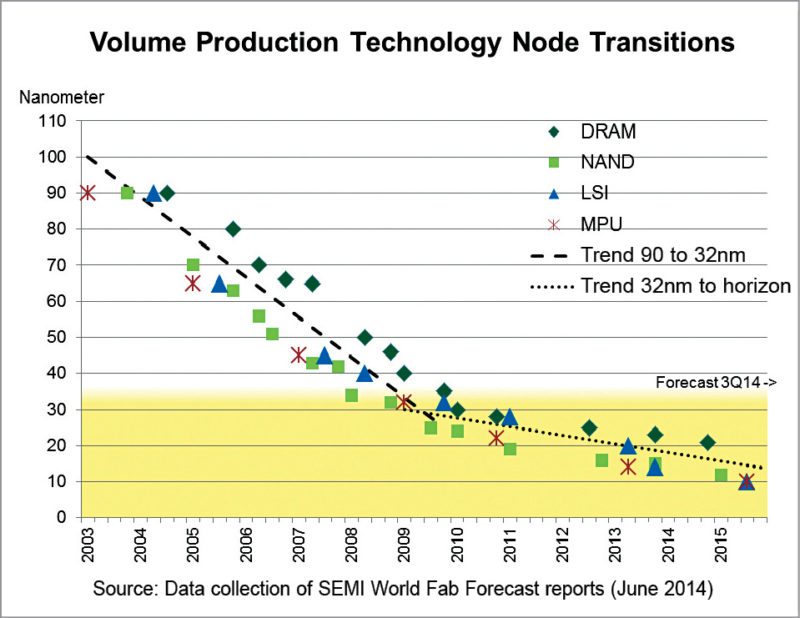
Because these are from the same group, indium and gallium have similar roles in chemical bonding. InGaAs is regarded as an alloy of gallium-arsenide and indium-arsenide with properties intermediate between the two, depending on the proportion of gallium to indium. InGaAs is a semiconductor with applications in electronics and optoelectronics. The graph in Fig. 3 shows 90nm, 65nm, 45nm, 32nm, 22nm, 14nm and 10nm to have around two years gap in every succession.
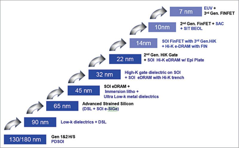
32nm/28nm was an inflection point below which it really was difficult to scale down. Double patterning and then multiple patterning started taking place. FinFET was invented, and now we are looking at gate-all-around and other innovative transistor structures, EUV and so on, to go below 10nm. Definitely, a few of these will have long maturity curves with major production volumes. It needs clever and strategic planning for fabs to reap the benefits from these; these would become cash cows in the long run.
Fabricating transistors is one part of the process, often called front-end-of-line (FEOL) process. Back-end-of-line process is for all interconnections, and there comes the complex part of managing resistance-capacitance.
Again, there are local interconnects at the device level, accomplished by middle-of-line process. Global interconnects are done by back-end-of-line and are prone to resistance-capacitance delays. Today, at lower nodes, back-end-of-line employs multiple patterning, which requires extra deposition and etching with every pattern, thus increasing the cost of production.
Technically, multiple patterning can still be viable at 7nm. However, the industry is looking at extreme ultraviolet (EUV) lithography to reduce that cost. With EUV, back-end-of-line process can be done with single exposure and throughput can be as good as ~150 wafers per hour. But for EUV lithography, foundries are dependent on semiconductor equipment manufacturing companies. It has developed a technology to fabricate test patterns with minimum line width of 1.5nm, which can be used to test metrological equipment with ultra-high precisions. Yield and patterning technologies are important.
Yield
Standard architecture of high-performance logic chips these days assumes that all transistors work, and we are talking about chips that would contain several billion transistors each. In terms of manufacturing and reliability, integrated semiconductor devices are amazing and put mechanical devices to shame—billions of components connected in a complicated way, and barring disaster, these things can all work for many years at a time without failure.
To be manufacturable, chip makers need to have the yield of good chips high enough to cover the manufacturing costs at a reasonable price point. That typically means yield rates over at least 30 per cent.
Patterning technology
All chips in recent years and even their prototype 10nm node products are patterned using photolithography, based on a light source with a wavelength of 193nm. Manufacturers have relied on pattern features down to one-twentieth of the free-space wavelength of light, including immersion lithography, optical phase control, exotic photochemistry and multiple patterning.
Finally, it is time to switch to a new light source of 13.5nm wavelength, which is the so-called EUV. This has been in the planning stages for years, with prototype EUV 300mm wafer systems. However, changing to new wavelengths and therefore new processing chemistry and procedures is fraught with challenges.
EUV lithography
EUV lithography represents a major technological advancement for semiconductor manufacturing. Current lithographic techniques utilise deep ultraviolet (DUV) light sources that produce wavelengths of 248nm or 193nm. EUV light used in EUV lithography has a wavelength of 13.5nm, a full order of magnitude shorter. This is important because imaging capabilities or resolutions of a lithography system are proportional to and limited by the wavelength of light used.
EUV remains a consistent challenge, and though manufacturers swear they can solve the power problem, the difficulties are staggering. Gate-all-around is an attractive method for improving transistor performance, but manufacturers are still struggling to hit reliability and dimension challenges. Materials like graphene or carbon nanotubes meanwhile would not debut for a decade or more in complex CMOS logic devices.
EUV light source produces short wavelength light in a system called laser produced plasma. Such light sources utilise a high-power laser to create high-energy plasma that emits short wavelength light inside a vacuum chamber. There are multiple ways that EUV differs, mostly associated with methods to create and transport the short wavelength light. Traditional lenses cannot be used with EUV as these absorb light. A mirror with a highly specialised coating, called multilayer mirror, must be used. Even these special mirrors absorb about 30 per cent of the light, so it is advantageous to use as few as possible. Any gas in the light path such as air or nitrogen will also absorb the light, thus the entire light path is inside a vacuum chamber. Primary EUV tool maker, ASML, projects EUV at 5nm node would require a higher numerical aperture than currently available and multiple patterning to a greater degree than immersion lithography at 20nm node.
Immersion lithography is still more than four times faster than EUV (275 WPH versus 65 WPH as detailed below), due to source power limitations. Hence, multiple patterning with immersion lithography has already been used where EUV had previously been expected to be used. However, it is currently recognised that EUV cannot practically realise 40nm to 50nm pitch due to stochastic effects in resist exposure, so even 10nm node is off limits. End of the road for silicon is nearing as alternative materials are now required for 7nm node and beyond.
Use of EUV lithography in a manufacturing plant today is almost as innovative as making 7nm SiGe based transistors. These use light in the DUV range at about 248nm wavelength to print 150nm to 120nm-size features on a chip. Beyond that point, smaller features require wavelengths in EUV range.
Light at 193nm and 157nm wavelengths is absorbed instead of transmitted by conventional lenses. The result is no light, no image and no circuit. To reach these small geometries, manufacturers use self-aligned quadruple patterning and EUV lithography. EUV lithography is a next-generation lithography technology using EUV wavelength, currently expected to be 13.5nm.
Current lithographic techniques utilise DUV light sources that produce wavelengths of 248nm or 193nm. EUV light used in EUV lithography has a wavelength of 13.5nm, a full order of magnitude shorter. This is important because imaging capabilities or resolutions of a lithography system are proportional to (and limited by) the wavelength of light used.
Read Part 2
V.P. Sampath is a senior member of IEEE and a member of Institution of Engineers India. He is a regular contributor to national newspapers, IEEE-MAS section, and has published international papers on VLSI and networks
