“Everything can be made in some way better—stronger, lighter, cheaper, easier to recycle—if it’s engineered and manufactured at the nanometre scale.” — Stan Williams director-Quantum Science Research HP Labs
JULY 2011: The 21st century can easily be called the era of portable devices that are lighter, smaller and a whole lot powerful in configuration than their predecessors. All this has largely been rendered possible with the size of the processor shrinking to the nanometre scale. These small-sized processors, also called microprocessors, have enabled the electronics manufacturers to build products that are smaller in size, have faster processing speeds and are powerful. However, experts view this development more as the continuation of existing microelectronics rather than a breakthrough in the nanotechnology space. They believe that this is merely a small application of nanotechnology and doesn’t represent even an iota of the potential that nanotechnology holds for the future of electronics.

Indeed, nanotechnology is not merely about reducing the size of processors to nanometres. Its domain is vast and still remains largely unexplored. Considering the research happening across the globe, and the advances so far in this space in terms of the development of new circuit materials and so forth, the technology surely holds a lot of promise for the technologists and electronics industry alike.
Apart from this, nanotechnology is being also viewed as a solution to the limitations of the current technologies. If we look at the current situation of digital electronics, there is presently no credible alternative to silicon complimentary metal-oxide-semiconductor (CMOS); all other technologies having failed to meet the standards of logic circuits. The improvements in silicon technology are also getting closer and closer to the ‘brick wall’ and this worries a lot of technology professionals and industrialists. It is anticipated that sometime around the end of this decade (2018 or so), it will become physically impossible to etch smaller features in silicon. Another challenge is that at lesser than 20nm sizes, silicon becomes electrically ‘leaky,’ which can cause short-circuits.
Is ‘nano’ the way to go?
With the current materials and technologies nearing the upper limit, scientists and researchers have built a lot of hope around nanotechnology, which according to them can help in developing alternative methods and materials. They believe that someday nanotechnology will revolutionise the global economy by providing power tools that will produce high-tech products using low-tech resources at low costs.
There is no denying the fact that on the concept level, nanotechnology holds a lot of promise. But in spite of breakthroughs prophesied in this field by many a scientist and futurist, especially if we consider the application of nanotechnology in the field of electronics, there hasn’t been much headway ever since the technology’s emergence in 1990s. In fact, the term nanotechnology has become more of a misnomer with different groups defining its periphery and scope differently.
To demystify the term and gauge the direction towards which the technology is moving, we turned to a few technology experts.
How much does ‘nano’ measure up in size?
Nanotechnology, which is sometimes shortened to ‘nano-tech,’ is the study of manipulating matter on an atomic and molecular scale. Generally, nanotechnology deals with structures sized between 1 to 100 nm in at least one dimension. It involves developing materials or devices possessing at least one dimension within that size. However, when it comes to the size, the opinions in the technology space are divided. There are some who claim that 45, 32 or 22nm technology does not qualify as nanoelectronics.
Vassilios Gerousis, senior architect, Cadence Design Systems, shares some of the varied viewpoints that are widely making rounds in the industry and amongst the science and engineering communities: “One opinion, which comes from the research fraternity deals with nodes that are between the dimensions of 10 nm and below, such as carbon tubes. Another opinion coming from the applied research domain caters to nodes between 14nm and 20nm. The third viewpoint is from the application side and is focused on 40nm and 28nm.”
Yet another view is that CMOS technology, even using nanoscale features, does not fully qualify as nanotechnology, because it uses mostly top-down fabrication to reach nanoscale dimensions. In this view, electronic devices should be labelled nanoelectronics only if these contain typical nanostructures such as carbon nanotubes or nanowires and dots. “However, the CMOS people themselves consider all technology nodes below 100 nm as nanoelectronics, since they comply with the basic definition of nanotechnology objects, i.e., structures with critical features below 100 nm,” says Marc Van Rossum, strategic adviser, Imec. “At Imec we share this view, and also consider several advanced top-down CMOS fabrication techniques such as extreme UV lithography and other nanoscale patterning tools to be part of nanotechnology,” he adds.
Considering that there are several possible definitions and opinions for ‘nano’ that have been used of late, the confusion has prevailed. “Nanoscale is commonly defined as smaller than 100 nm and, by that definition, modern electronics have been at nanoscale for about a decade. This is the definition that Intel uses,” quips Michael Mayberry, director—components research, technology and manufacturing group, Intel.
A competing definition typically used for nanomaterials is to count both size and process for fabrication. Here some insist that making larger objects smaller doesn’t count and you should only count those using bottoms-up methods.
Clearing the air on the subject, Dr Denis Koltsov, consultant in Nanotechnology, BREC Solutions (UK), says, “Unfortunately, there is a lot of misunderstanding of the term ‘nano’ in whole of the nanotechnology community. The subgroups like nanoelectronics seem to deviate from an official ISO definition of nanotechnology if they are claiming that 45-22nm technology is still not nano electronics. Any device that is smaller than 100 nm in at least one dimension would be classed as nano-device. This also applies to thin-film devices like hard disks. While it is (understandably) difficult to call a big hard disk a nano electronics device, it is definitely not correct to reject a 22nm technology from nano-electronics community by definition. A much more appropriate definition for those that work with molecules and nano tubes would be molecular electronics or pico technology (1nm-0.1nm size). Please note that these are not ISO definitions.”
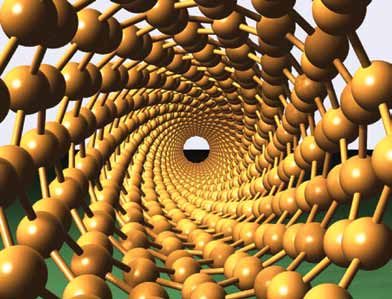
Dr James Canton, futurist, adviser, CEO, Institute for Global Futures www.FutureGuru.com, and author of the book Extreme Future, adds another perspective, “People think that nano science is about size, while it is more about capturing in small platform a dense amount of functionality and performance.” Also, nano is about changing the concept of synthetic consciousness in developing other forms of intelligences that can function at the quantum level.
How far is nano from going mainstream in electronics?
Going beyond the concept, let us now look at the way nanotechnology has evolved in the last one decade and the direction towards which it is heading.
If we look at the application side, it is believed that most of the nanoelectronics technologies (at the transistor level) demonstrated today—such as hybrid molecular/semiconductor electronics, one dimensional nanotubes/nano-wires and advanced molecular electronics—are futuristic and not usable anytime in the near future. As a general statement it is true. The industry has had its share of doubts about the wide scale adoption of nano-technology in electronics. Currently, in the mainstream we see 40nm and 28nm technologies, says Gerousis. Most of the work that is underway below the 20nm dimension is in the research and development phase.
The key challenge that is being faced by the industry and researchers is that while the nanomaterials are exotic, these are not easy to produce. Some of the exotic nanomaterials, including carbon nanotubes, have very interesting proper-ties as materials. But the industry still lacks the ability to precisely form and use them for electronics where we typically need to fabricate billions of transistors at once, opines Mayberry.
“The largest of the exotic material demonstrations have been of the order of a handful of devices working together. Nevertheless, considering the pace of science and technology advances, I think eight to ten years from now we might be using some of these exotic materials in electronics production. For applications requiring less precision some of these nanomaterials are already in use,” he adds.
Devices using carbon nanotubes or nanowire transistors show promise for specialised sensors, and there is also some perspective for nanowire solar cells. But molecular devices have only proven their relevance at the diode level, and a genuine single molecule transistor (three-terminal device) with acceptable characteristics is still out of reach.
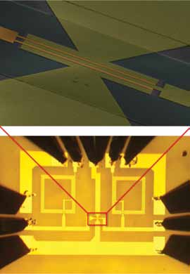
“Nanoscale spin transistors are also interesting, but they exist only at the exploratory level. In any case, those devices still require huge break-throughs in many challenges such as reproducibility, dimensional control, positioning, contacts, doping and transport properties in general. At this time, none of these technologies has a proven advantage over CMOS,” Rossum avers.
But it is equally true that all nano-techniques, which are compatible with CMOS, are worth considering to over-come the bottlenecks related to lithography, such as power dissipation and leak-age, signal transmission speed and integrity, adds Rossum. “The goal is to push CMOS node scaling-down to 16 nm, 11 nm or even below. At 11 nm there will still be no need for CMOS alternatives. However, below that scale the situation is less clear. It has sometimes been stated that molecular or atomic devices would offer many attractive features, but the truth is that in conventional electronics the laws of quantum mechanics work against us once we reach the quantisation level,” he opines.
So, where does the paradox lie? Why a technology that is so promising at the concept level has failed to scale up when it comes to its mainstream application in the electronics domain? Enumerating a few reasons, Kolstov says, “The research in molecular nano-electronics is unfortunately very sensational. What I mean is that a research group may measure some effect from one device and write a very popular paper. However, this result has limited use for industrial community since it may not be reproducible, and in some cases is simply wrong. Some recent publications (http://www.nanotechia.org/global-news/is-there-plenty-of-room-at-the-bottom-for-nanomanufacture) argued that some applications of nanoelectronics may never be manufacturable.”
“If we look at the developments so far, it won’t be wrong to say that nanoscience is both futuristic and here today,” affirms Dr Canton. While it is true that the progress made so far in this domain has still not been too fruitful, yet there are areas where the application of nano-science has led to interesting results. Dr Canton enumerates, “Molecular electronics have been shown in the Quantum Computing Lab of Stan Williams at HP to be possible. IBM has done extensive work in nano computer chip development that will likely extend silicon’s life as a chip platform. Mercedes uses nano on coatings for autos to protect the driver. Having said this, nano is emerging and the potential is great, but it is in the early stages.”
Looking beyond processors…
The relevance of nanotechnology and nano materials for reducing the size of transistors can’t be ignored. “Carbon technologies using carbon nanotubes (CNTs), graphene or other allotropes are becoming more and more relevant in this race to continue the Moore’s law,” opines Dr Denis Koltsov. But it would also be worthwhile to explore a few other areas in the electronics space where nanotechnology can potentially have its influence. Let’s take a look at a few of such domains.
Digital displays. The quality of digital display screens in electronic devices can be improved by reducing the power consumption while decreasing the weight and thickness of the screens. Nano research projects are underway to make use of electrodes made from nanowires to enable flat panel displays, which are likely to be a lot more thinner than the current flat panel displays. “CNTs, which are up to 100-times stronger than steel, and yet only one sixth of its weight, are also being used to direct electrons to illuminate pixels and to develop light-weight, millimeter thick ‘nanoemmissive’ display panel,” informs Rossum. A company called Rosseter in Cyprus is already producing them for commercial use because of their rugged chemical, physical and mechanical properties.
MIT researchers have also created a quantum dot-organic light emitting diode (QD-OLED). While the traditional LCDs are lit from behind, the quantum dots have the capability of generating their own light, and these dots can be manipulated to emit any colour imaginable, with no range limit as seen with traditional devices.
For larger memory sizes. With consumers demanding electronic devices such as music players, mobile phones and computers with gigabytes of memory, the future electronics devices will surely need even larger memory sizes. “The current storage technologies, like Flash memory technology, has an upper-size limit as well as a rewrite limit (between 10,000 and 100,000 writes). Thereafter it will no longer be able to store data. To gear-up to meet with this requirement, multiple examples of memory technologies are being explored that use more exotic materials than what is used in production today,” says Mayberry.
Nanosized magnetic rings are being tried to make magnetoresistive random access memory (MRAM), which research has indicated may allow memory density of 62 GB per square centimetre (400 GB per square inch). Research is also on for using microelectro-mechanical system (MEMS) techniques to control an array of probes, whose tips have a radius of a few nanometres. These probes are used to write and read data onto a polymer film, with the aim of producing memory chips that have a formidable density. There is also ongoing research for the use of nanosized ‘dots’ of nickel, which it is hoped could be used to store terabytes of data, even for home and personal users.
Rossum says, “There are many ideas of using nano features in non volatile memories—molecular structures, metallic nanodots, organic molecules, nanostructured materials and so on. Although their applications are not yet mature, it is still an interesting avenue of research.”
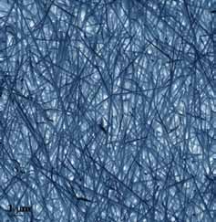
In making existing technologies better. “The developments in nano-technology as a sector have already shown us that this new technology is not only about doing things better, faster at a smaller scale, but also about adding new functionality to existing technologies,” says Kolstov.
“The devices, sensors, etc, are gaining another option, like, for example, the development of Spin-FET. In that case the charge and spin of the electrons are used to offer novel functionality. I think the advent of CNT electronics applications, Spin-FETs and properties of graphene are the hottest topics in industry at the moment. I am sure this may change, but in the meantime there is a lot to research in those areas,” he adds.
For healthcare and environment. Nano today is about size and material science innovations. In the future it will be about designing matter at the atomic level to address climate change, hunger, war, healthcare and energy needs,” believes Dr Canton. In the future, convergence of nanoelectronics with bioelectronics could be important for health and comfort applications, provided the technology becomes affordable. “Already, nano wires are being used to restore movement in crippled legs, by restoring neural path-ways to connect the brain to the body for movement,” informs Dr Canton. A few more possibilities include nano-energy development or storage, nano-geoengineering to clean up the planet, nano-machines to enhance the food supply to resolve world hunger, nano-intelligence to enhance humans and to use nano-devices to deliver drugs or medicines to help heal people.
Faster data transfer between devices and networks. According to nanoforum.org, optoelectronics can help in dramatically increasing data transfer rates within devices like PCs by replacing the existing copper wiring. Instead, in the future, quantum dot-based lasers may also be used to transfer information between components within devices at the speed of light, with each piece of information ‘coded’ using a unique wavelength of light.
If we look at external networks, data transfer can take place more rapidly between two points if we increase the number of nodes in information networks. This will become possible through the development of cheap ambient-sensor networks based on nanotechnology, and will help the telecommunication sector to achieve better data transfer rates.
Circuits for wireless devices. IBM Research scientists recently announced the first integrated circuit fabricated from wafer-size graphene, and demonstrated a broadband frequency-mixer operating at frequencies up to 10GHz (10 billion cycles/second). Designed for wireless communications, this graphene-based analogue integrated circuit (having the thickness of an atom) could improve today’s wireless devices and points to the potential for a new set of applications.
At today’s conventional frequencies, cellphone and transceiver signals could be improved, potentially allowing phones to work at places where they can’t today. While, at much higher frequencies, military and medical personnel could see concealed weapons or conduct medical imaging without the radiation dangers of X-rays.
“Nano is fundamentally a convergent science. Nano-Neuro-Bio-IT-Quantum all together as the top convergent sciences will transform the future of our world and our planet for the better,” foresees Dr Canton. Going forward, the nanotech enterprises will provide the ultimate convergence of computers, networks and biotech, and create products never before even imagined.
Other than the present uses for coatings, materials or components to achieve a smaller size, he foresees a few more areas where the technology may eventually have useful application. He says, “Future applications are for self-assembly of energy-on-demand for devices, robot bodies to morph to adapt to the environment or the job. Nano memory metal has attributes of body morphing. Time/space transformation, the development of neuro-brains to augment device intelligence or to augment human and machine intelligence are a few other interesting application areas.”
Going forward
While it won’t be wrong to say that we are still far from unleashing and leveraging the true potential of nanotechnology, the progress made so far in the science research labs and industrial R&D units is encouraging. These developments point to the fact that nanotechnology is truly going to be the key technology that will usher in an industrial revolution of the 21st century. Quoting the words of Michiharu Nakamura, executive VP at Hitachi, “…those who control nanotechnology will lead the industry.”
Vandana Sharma is executive editor for EFY’s Linux For You magazine, while Janani Gopalakrishnan Vikram is a technically-qualified freelance writer, editor and hands-on mom based in Singapore


