Everyday gadgets that we use employ highly miniaturised circuits and if you ever ‘accidently’ opened any such device, you know we cannot etch a processing chip on any regular Printed Circuit Board (PCB). These require clean rooms and sophisticated equipment. Such manufacturers, in essence, are the unsung heroes behind the large-scale adoption of technology.
Making basic components like Integrated Circuits (IC) for electronic devices is an art in itself. After all these ICs are what rules the phone in your hand or the computer on your desk. Let’s take a look into the process behind such wondrous manufacturing.

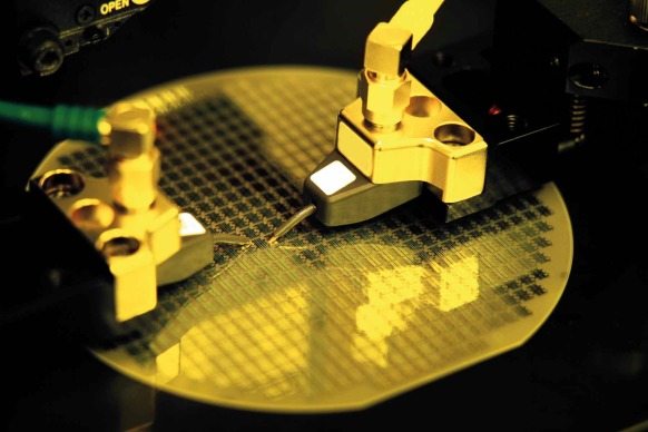
Steps involved in making an IC
Making an IC is a very complicated process and high care is taken to get everything right. Even a single dust particle can cause a short circuit in the equipment.
1. Cleansing
A single wafer goes through very stringent cleanliness measures in order to make the perfect solution. Even before involving the hardware, we have several steps to check for any problems that may occur in the finished product. Once those are taken care of, we are fabricating the hardware.
2. Wafer preparation
The wafer is first prepared for fabrication by converting an ingot (cylindrical block of silicon) into thin strips of about 0.004 to 0.01 cm. These would later provide to be the base of the IC. After clearing for any scrapes, this wafer is subjected to superheated steam at about 1000 C. This creates an insulating coating of Silicon DiOxide (SiO2) to prevent any unwanted oxidation of the silicon that would cause problems later on.

3. Masking
Then the wafer goes for masking. Here the wafer is coated in a photoresist material. Once the wafer is completely coated in photoresist material, the process of exposure under Ultra Violet (UV) light takes place. Here, the wafer is exposed to UV light such that the photoresist material is differentiated in the form of hard and soft material. Next comes etching out the excess/unwanted silicon. The unwanted silicon is removed along with the excess photoresist material. Now we have the required circuit on a wafer.
4. Doping
Next, we have doping and other ion implantation on the wafer. This is done in order to create transistors and such similar circuit components on the wafer. Once this is completed, a mechanically operated fine diamond cutter cuts the wafer. This creates several ICs from a single wafer of Silicon.
After several quality and other checks, the appropriate connections are made. Now we have a completed IC that can be packaged as required.
 How do they do it?
Once we know the steps taken to manufacture an IC, a question that comes to mind is about the tools involved in the entire process. These have to be specialised tools with superior quality and durability. The machines involved into making these wafers cannot be changed regularly with each new update, so they have to be able to perform highly complex tasks with regular support from the manufacturer. But we never hear of these equipment, or their manufacturers.
Developing the equipment
 A lot of research goes into making these equipment, as these are not easily replaceable. Additionally, “We also provide refurbishing with our equipment. We take our equipment and make suitable modifications making them ready to handle the evolving demands of the industry,” adds Ashok Belle, MD, Lam Research India.
The designing of these systems in done entirely within the organisation through Offshore Development Centres managed by firms like LAM Research. “We do research in collaboration with the customers. This makes way for the proper and desired equipment to be developed,” says Belle. The constant advancements in technology demands the need for machines that are both efficient and accurate in their delivery. The research done helps in bringing the equipment that the users want, and not just adding random features.
Equipment Quality and Employment
For a fabrication lab to be successful, it has to work at almost full potential. Anything less causes a dent in the manufacturing target and has to be taken into consideration. There are also a large number of fabricated chips being rejected after the quality and electricity checks. All these factors determine the final output. These machines have to be state of the art to provide maximum throughput in order for the fabrication labs to be successfully produce IC and other components.
Using such specialised equipment requires trained professionals, as you would not want an ingot turn into scrap overnight. “Exclusive training is provided with new equipment. A dedicated 24×7 support centre is also available with our products,” adds Belle.
Fabrication status in India
LAM Research is a manufacturer of fabrication equipment with a very significant market share. Hence, they are in a good position to comment about the fabrication sector in India.
With the setting up of such a big time firm in India comes the question of the Indian market. Today, in India we have all of the wafer related products being imported from outside. According to Belle, “Most of the steps are done in controlled atmosphere or clean room in US. Here (in India) we have developers focusing on the designing, of those equipment.”
This causes limited products being called into the continent, as no supplier would supply 20 ICs internationally without a hefty transport charge. This filter allows only the well-established and promising ICs to be available in India.
A couple of years ago, steps were being taken to remove this dependence, and there were talks of establishing some fabrication labs in India. This would have provided a boost to the Indian semiconductor industry while putting fabrication equipment manufacturers on the Indian map. The government extended the deadline for submission of documents up to April 30, 2016, stating that, “They are yet to submit some ‘other documents’, which are considered essential to demonstrate their commitment to the projects.” Such bottlenecks can often cause long delays in the proposed timeline.
A collaboration of industry veterans Lou Hutter and Mark Harward, Cricket Semiconductor is expected to start work on setting up a fabrication plant (fab) in Madhya Pradesh by Q2 2016. The plant is expected to be operational by 2018. Industry experts expect the analogue fab to operate on 180-130 nm technologies. Also, since large economies of scale are required to drive down costs, this fab is slated to produce 60,000 wafers per month. At this sort of volume, the fab could become cost competitive compared to the digital fabs. This could very well prove to be the very step in redefining electronics in India, while taking the Make in India initiative to new heights.
Welcome to the future
With Moore’s Law going to the wolves, there is going to be an ever-increasing growth in electronics design. “Technology is moving at a very fast pace. Now we have microSD cards with 64 – 128 GB storage. This calls for state of the art equipment that we provide,” adds Belle. Such design would always require equipment capable of working with high accuracy. This would always keep such fabrication equipment designers on their toes, working on bringing in the next “it” product.
By Saurabh Durgapal with inputs from Mr. Ashok Belle, MD, Lam Research India