


Sometimes it is the applications that drive a technology. We can look at ‘Big Data’ as one of the reasons why the spotlight is back on solid-state storage technology. Solid-state storage is not new. This silicon based electronic method of data storage has been around for a long time now. As ‘memory’ to speed up transactions between processors and hard disk drives, and then as ‘storage’ in smaller devices like mobile phones, solid-state storage has proved to be useful. It has also been used for mission-critical applications like defence where speed is imperative. However, with a splurge in Big Data brought about by the Internet of Things (IoT) devices and enterprise applications, the need for faster storage is felt more than ever—giving rise to the development of mega-sized solid-state drives (SSDs) and increased research on how to make larger SSDs at a lower cost. While we might have thought it impossible some years back, online marketplaces show that it is now possible to buy a two-terabyte (TB) peripheral component interconnect express (PCIe) based SSD for less than US$ 3000 and a 1TB one for US$ 500-1000. So we might not be entirely wrong in hoping for a future of data centres populated entirely with SSDs!

Terabyte-scale storage sees uptrend (literally)
The industry has been steadily increasing the capacity of flash memory by reducing space wastage, but still there is only so much you can store on a piece of silicon! However, even at a stage when it is difficult to reduce the cells’ pitch size further, the capacity of SSDs continues to go up, thanks to technologies that enable cells to be stacked one above the other. In 2015, all the industry majors ranging from Intel Corporation and Micron Technology, SanDisk and Toshiba, to Samsung, unveiled prototypes that involved stacking of flash cells.
Basically, one of the ways in which flash memory has evolved in the past deals with the number of bits stored per cell. The earliest were single-level cells (SLCs) that stored one bit per cell, followed by multi-level cells (MLCs) that stored two bits per cell, and then triple-level cells (TLCs) that can store three bits per cell. Although storing more bits in a cell made flash memory cheaper and capable of storing more data, it was not very reliable. Overall, SLCs were found to be faster, more durable, reliable and power-efficient for large enterprise-scale applications. Last year, Intel and Micron revealed a new three-dimensional NAND (3D NAND) technology that uses MLC and TLC technology to bring down the cost of storage, while also promising enough reliability and power-saving for large applications.
Here, flash cells are stacked vertically in 32 layers to achieve 256-gigabit (32GB) MLC and 384-gigabit (48GB) TLC dies that fit within a standard package. According to the press release, this enables three times the capacity of existing 3D technology—up to 48GB of NAND per die—enabling three-fourths of a terabyte to fit in a single fingertip-size package. So a small gum-stick-size SSD can hold more than 3.5TB of storage and a standard 6.35cm (2.5-inch) SSD can accommodate more than 10TB. Since the growth in capacity is achieved by stacking the cells and not by bringing down their dimensions, both performance and endurance are increased, making even the TLC designs suitable for data centre storage.

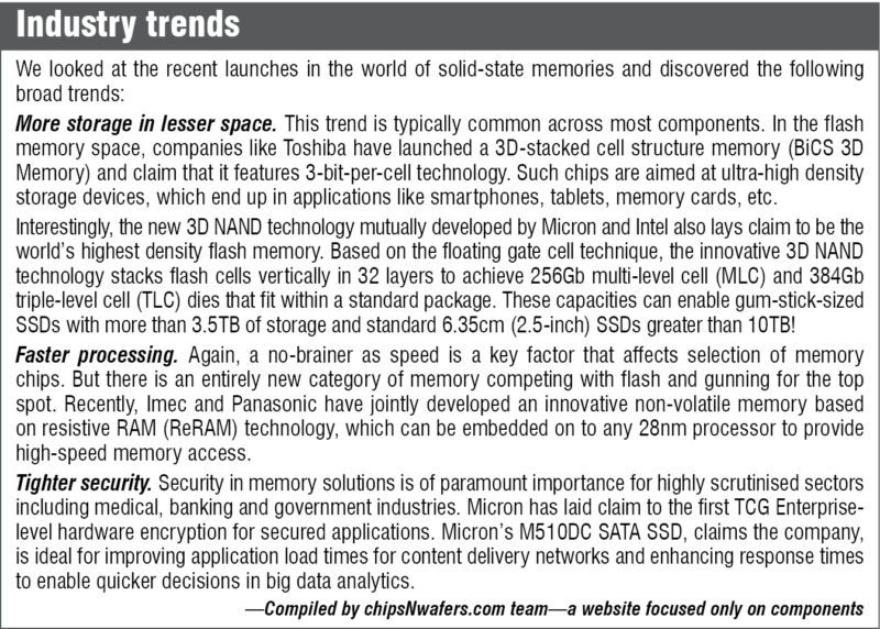
Another innovation that helps increase the performance and reliability of this 3D NAND flash memory is the use of a floating gate cell design. In this architecture, the cells’ transistors have a second insulated gate that retains the electrons till a strong external voltage is applied. This is a time-tested method frequently used in 2D NAND flash, which Intel has extended to their 3D design, too. Other features like sleep mode are also incorporated in the design to enable power savings, too.
SanDisk, in association with Toshiba, has also developed a 256-gigabit 3D NAND chip, with three bits per cell and 48 layers.
Samsung’s three-dimensional vertical-NAND (3D V-NAND) technology has enabled it to make a 6.35cm SSD of around 16TB capacity. V-NAND involves both structural and material innovations. A new technology called the Channel Hole Technology enables the stacked cells to connect vertically through a cylindrical channel that runs through these. This is supplemented with a material innovation called the Charge Trap Flash technology, which prevents data corruption caused by cell-to-cell interference. This technology uses a non-conductive layer of silicon nitride, which wraps around the control gate of a cell, acting as an insulator that temporarily traps electrical charges and maintains cell integrity. While current products and prototypes have 48 layers, Samsung says its technology is capable of 100 layers, which it hopes to achieve by 2017.
In March this year, Samsung officially announced the launch of PM1633a, a 15.36TB drive, for enterprise applications. The SSD is based on a 12-gigabit-per-second serial attached SCSI interface and comes in a 6.35cm form factor.
Keeping up with the networks
The latest networking standards seem to promise nothing short of lightning speed. The emerging Wi-Fi standard 802.11ac operates at 1300Mbps, Wi-Gig (802.11ad) that was introduced in Intel’s sixth-generation Core PC platform can operate at 7000Mbps, universal serial bus (USB) 3.1 at 10,000Mbps and Thunderbolt 3 at 40,000Mbps. Hard disk drives (HDDs) are hopelessly slow in comparison, and that is why no one imagines future personal computers to have these.
SSDs fare much better than HDDs, but even the current-generation serial AT attachment (SATA) SSDs—that typically have speeds of about 4400Mbps—do not seem any match for the latest networks. What is to be noted here is that, the NAND flash memory is not the bottleneck but the SATA interface is. In order to overcome this, the industry has standardised on a protocol called non-volatile memory express (NVMe) that communicates over the PCIe host interface. NVMe is considered to bode well for the SSD industry because this technology has been developed for solid-state storage, which means a lot of parallelism and other exceptional features have been designed into it. Plus, standardisation of this technology will eventually drive down the cost, making SSDs more affordable to everybody.
The NVMe interface scales up by using multiple lanes. For example, an NVMe SSD with four lanes has a speed of 32,000Mbps, which is many times faster than SATA SSDs. While SATA supports a single queue of up to 32 commands, NVMe supports 64,000 queues that can each hold up to 64,000 commands.
Let us say, you have a quad-core computer. NVMe will enable commands to be completed in parallel across all the four cores, while in the case of SATA the commands have to go through a single core. That way, NVMe increases throughput and reduces latency. With an NVMe SSD and a fast network connection, data sharing from your laptop will be super-fast. Experts feel that the speed of NVMe SSDs will also extend a laptop’s battery life. If you take the example of a data transfer job that requires an HDD to operate at an active power of 6W for 180 seconds, an NVMe SSD can complete the same task in 10 seconds. This means 6W of active power for just 10 seconds, after which it reverts to idle power.
NVMe SDDs will also reduce the footprint and power consumption of large data centres, because on an average 10 SATA SSDs can be replaced with one NVMe SSD.
In the big league
Of late, we are seeing many key players launching all-flash solutions for large data centres. Trend-watchers note that enterprise and cloud players are beginning to consider flash based solutions not only for hot storage but for cold storage as well! No wonder 2016 is seeing a lot of activity on this front.
EMC recently launched the VMAX All Flash, a solution for mission-critical enterprise data centre applications, which it claims is more cost-effective than traditional methods. The all-flash storage array natively supports block, file, open systems and mainframe. VMAX All Flash includes innovative technologies such as Write Folding to improve flash durability while simultaneously delivering peak performance.
In March, Seagate demonstrated a new PCIe flash drive, which meets the Open Computer Project (OCP) specifications and delivers throughput of 10 gigabytes-per-second (GB/s). The add-in card bundles multiple small-sized, energy-efficient, consumer-grade M.2 SSDs. It accommodates 16-lane PCIe slots and supports NVMe. Seagate’s new solution includes capabilities like bifurcation of PCIe lanes at boot-up, out-of-band temperature and performance measurements, and the management of airflow and fan control in out-of-band fashion, in order to comply with OCP specifications. OCP, an initiative driven mainly by Facebook, is a collaborative effort to redesign hardware to meet the increasing demands on IT infrastructure, especially in large data centres with thousands of servers.
All-new tech, considered as new category
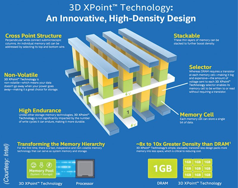
Although Intel Corporation and Micron Technology have showcased some 3D NAND designs, it is clear that they are betting on something bigger for the future. They go so far as to call their 3D XPoint technology the first new memory category since the introduction of NAND flash in 1989!
Demonstrated last year, 3D XPoint technology is a non-volatile memory that can provide extremely fast access to large sets of data. It is thousand times faster and thousand times more durable than NAND, and ten times denser than conventional memory. According to an Intel press release, “An innovative, transistorless cross-point architecture creates a three-dimensional checkerboard where memory cells sit at the intersection of word lines and bit lines, allowing the cells to be addressed individually. As a result, data can be written and read in small sizes, leading to faster and more efficient read/write processes.”
Picture 128 billion densely-packed memory cells, connected with perpendicular conductors. These cells store a single bit of data each, and can be accessed and written or read by varying the amount of voltage sent to each selector. The storage parts and the selector will be made of special chalcogenide materials. Unlike NAND, which works by trapping electrons in the cell, here writing to the drive will fundamentally change the actual material of each memory cell. This new physical concept, along with the transistor-free cross-point architecture, gives Intel’s 3D XPoint tech an enviable combination of high density, capacity and performance at a low cost. While current versions of the technology can store 128 gigabits per die across two stacked memory layers, in the future it is possible to increase the number of memory layers as well as increase die capacity using traditional lithographic pitch scaling.
This year, the company might bring to the market a new line of SSDs based on Intel Optane technology, which will combine 3D XPoint with an advanced system memory controller, interface hardware and software intellectual property. Intel dual-inline-memory-modules based on XPoint are also on the anvil for the data centre.
According to some expert reviews, XPoint chips can deliver more than 95,000 input/output operations per second (IOPS) at a 9-microsecond latency, compared to 13,400 IOPS and 73ms latency for flash in an NVMe based SSD. While that triggers awake our wildest dreams, there are also some constraints to think about, as Guy Blalock, co-CEO of IM Flash (the semiconductor company founded by Intel and Micron) pointed out at the Industry Strategy Symposium hosted by the SEMI trade group.
One possible problem with the new materials used in the design is their potential for cross-contamination. To mitigate this, they have to develop a lot of process steps for layer-over-layer deposition with a lot of diffusion and chemical vapour deposition. Plus, the 100+ new materials used by 3D XPoint also raise supply chain challenges. The design also requires more machines running process steps, cutting fab throughput by an estimated 15 per cent. This could increase capital expense and space needed by three to five times compared to new generations of flash. However, the company believes XPoint is the future and it is likely to iron out all these issues within the next few months, so we can still hope to see personal computer and data centre products based on this revolutionary tech. In fact, rumours are that Intel’s Optane SSDs might make their way into the next MacBook.
Non-volatile memristor memory
Around two years back, Hewlett Packard Co. announced that it was working on a futuristic and nothing short of revolutionary computer called The Machine, which is to be made of specialised computing cores, photonic connections and an extremely dense, energy-efficient memristor memory. The Machine, now being developed by HP spin-off Hewlett Packard Enterprise (HPE), would be able to handle petabyte-scale data sets as if it were child’s play.
The memristor memory part is what we hope has caught your attention now. Memristor memory is a non-volatile memory that uses memristors or electrical components that regulate the flow of current in a circuit and remembers the amount of charge that has previously flowed through it.
If Intel bets the future of SSDs on 3D XPoint, HPE has its hopes for memristor memory. HPE and SanDisk have now partnered to develop a new storage class memory technology, which will combine the best of HPE’s memristor project and SanDisk’s non-volatile resistive random access memory (ReRAM) technology. ReRAM, too, is a memristor based technology.
Rough sketches show that the design will involve tiny conductive filaments crisscrossing and connecting silicon layers to represent a bit of data. The resulting non-volatile memory technology is expected to be up to thousand times faster and thousand times more durable than current flash technology. (This is exactly what Intel says about 3D XPoint, so we can well assume that this is how SSDs of the future will be!) It will be byte-addressable like DRAM and will allow systems to employ several terabytes of storage class memory cache per server node for large-scale applications. The resulting technology will be used not only for The Machine but also to make other commercial and enterprise products.
Other companies are also working towards commercialising ReRAM technology by this year. One such is Silicon Valley start-up Crossbar, who hopes that some of their 3D Restive RAM products will be used as memory in wearable devices this year, and in high-density SSDs sometime next year or later.
Looking further into the future
There is a lot of exciting research happening at universities, which hint at what is in store for SSDs well into the future. Here are some examples:
Tantalum based memory. One such research was revealed by scientists of Rice University last year. A team of chemists led by James Tour discovered that applying a voltage to a 250-nanometre-thick sandwich of graphene, tantalum, nano-porous tantalum oxide (an insulator) and platinum creates addressable bits where the layers meet. Control voltages can be used to shift oxygen ions and vacancies, to switch the bits between ones and zeroes. The team used this to create a solid-state memory technology that allows for high-density 162-gigabit non-volatile storage. The new devices require only two electrodes per circuit, which is simpler than current-generation flash memories.
According to Tour’s comments in the university’s press reports, “This tantalum memory is based on two-terminal systems, so it’s all set for 3D memory stacks… And it doesn’t even need diodes or selectors, making it one of the easiest ultra-dense memories to construct. This will be a real competitor for the growing memory demands in high-definition video storage and server arrays.”
Further, the tantalum oxide memories can be fabricated at room temperature. The control voltage for write/rewrite is adjustable, allowing a wide range of switching characteristics. The main challenges in the way of commercialising this memory technology are the fabrication of a crossbar device dense enough to address individual bits and a way to control the size of the nano-pores.
BlueDBM. Although not an SSD technology by itself, BlueDBM, an ongoing project at the Massachusetts Institute of Technology has the potential to improve the usage of upcoming flash based storage technologies. A system architecture to accelerate Big Data analytics, BlueDBM comprises a large distributed flash based storage with in-store processing capability and a low-latency high-throughput inter-controller networks.
In some Big Data scenarios, performance is affected by the capacity of fast local DRAM, and in cluster systems with more RAM, the network stack ends up being a bottleneck. BlueDBM attempts to overcome these issues by providing extremely fast access to a scalable network of flash based storage devices, and to provide a platform for application-specific hardware accelerators on the data path on each of the storage devices.
According to the project overview, “Each BlueDBM node consists of flash storage coupled with a field-programmable gate array (FPGA), and is plugged into a host system’s PCIe port. Each node is connected to up to eight other BlueDBM nodes over a high-speed serial link capable of 10-gigabit bandwidth at 0.5µs latency. By default, the FPGA includes platform functions such as flash, network and on-board DRAM management and exposes a high-level abstraction.”
Photonic memory. In a paper published in nature.com last year, a group of scientists from English and German universities proposed an integrated all-photonic, non-volatile multi-level memory. Photonic data storage can greatly improve the performance of computing systems by reducing the latencies associated with electrical memories and potentially eliminating optoelectronic conversions. While scientists have experimented with photonic memory earlier, these attempts mostly resulted in volatile memory.
The recent breakthrough uses phase-change materials to achieve a robust, non-volatile, all-photonic memory. In simple terms, this solution uses waveguide technology to move light from lasers across a germanium, tellurium and antimony alloy nano-coating. The structure of the alloy is altered in predictable patterns when hit by light from a high-intensity laser. A low-power laser is used to read the patterns and translate it as data. By using optical near-field effects, the team has achieved bit storage of up to eight levels in a single device that readily switches between intermediate states. According to the paper, the on-chip memory cells feature single-shot readout and switching energies as low as 13.4pJ at speeds approaching 1GHz.
Before they think of commercialisation, the team has to figure out how to reduce the size of their prototype, which is much larger than current-generation memory chips! However, in terms of performance, photonic memory can easily outperform SSDs, so it is a worthy pursuit.
SSDs cannot be monarchs
Speaking on the future of SSDs at last year’s SNIA Storage Developer Conference in Santa Clara, California, Jim Handy from Objective Analysis said, “Future memory and storage systems will include everything: DRAM, non-volatile memory, NAND and hybrid hard drives. One technology will not kill off the others.”
Jim added, “The result of all the changes in technologies and architectures is a new component: storage-class memory. This memory will combine the benefits of a solid-state memory with DRAM performance and robustness and archival capabilities and low cost of hard-disc magnetic storage. The persistent memories will disrupt the entrenched thoughts on possible and available latency budgets for storage… The computer of tomorrow will have fixed DRAM size made of stacked packaging of DRAM dice, and upgradeable non-volatile memory that will be the equivalent of DIMMs. The storage system will include both flash and disk with the flash on PCIe of its own bus. The magnetic drives will continue to exist for mass storage as there is no foreseeable price crossover for high-density, long-term storage. Finally, the storage class memory software will eventually get to the point where is will contribute to overall system performance.”
So it is clear that, while we will see more SSDs around us in the coming years, an all-flash era might be quite far away.
Like this article? You may also like other Tech Focus articles
Janani Gopalakrishnan Vikram is a technically-qualified freelance writer, editor and hands-on mom based in Chennai