Where does India’s electronics dream stand when it comes to the reality of execution? At the EFY Expo Gujarat 2025, the industry united to unpack what India must fix: IP, fabs, EDA tools, skills, to truly lead the global ESDM race.
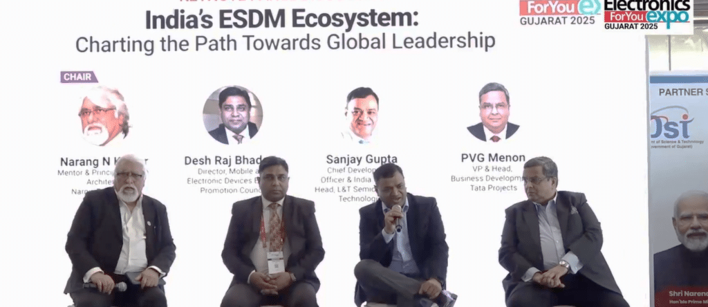
In India’s electronics story, momentum is no longer in question; direction is. Exports are rising, manufacturing capacity is expanding, and policy frameworks are aligning with long-term strategic intent. However, a more fundamental question is emerging across the industry: with rapid growth heavily reliant on imports and minimal local value creation, who ultimately captures the economic benefits?
“India is at an interesting juncture,” observed Narang N. Kishor from Narnix Technolabs, pointing to the structural shifts triggered during the COVID-19 period. “Crises often present the greatest opportunities.” As global supply chains recalibrate and countries reassess dependencies, India finds itself at the centre of a rare opening. “As the world looks to reduce economic dependence on China,” he added, “the question is whether India can position itself effectively in this evolving landscape.”
The opportunity is real. But opportunity alone does not create leadership.
The limits of assembly-led growth: Is the market expanding faster than its value capture?
The scale of India’s electronics market is no longer in doubt. What remains uncertain is how much of that value will stay within the country. “We are at a critical inflection point for the country,” said Sanjay Gupta of L&T Semiconductor Technologies. “In many ways, we are fortunate not only to witness this moment, but also to contribute to it.”

India’s electronics consumption is projected to reach $300 billion and eventually $500 billion. “At some point, this could even surpass oil imports,” he noted, drawing a parallel that carries both promise and risk. “If left unaddressed, like oil, it could significantly drain the economy.”
At the core of this consumption lies semiconductors, the highest-value component in electronic systems. “Semiconductors represent roughly 30-40% of the value,” Gupta said. Current consumption stands at $40-50 billion, with projections of $100 billion by 2030. The numbers point to growth. But they also expose a gap.
Now the point is, the value sits elsewhere.
The gap becomes clearer when viewed through the lens of product economics. “Take a smartphone, even a premium device priced above $1000,” Gupta explained. “The reason for that value lies in innovation, unique hardware, chips, and embedded software. Without these, the physical manufacturing cost might be just $100–300.”
The implication is stark. “So, 70-90% of the value comes from design, innovation, and intellectual property,” noted Gupta.
India’s rise in manufacturing, particularly in smartphones, has been driven by assembly and integration. These are necessary capabilities, but they capture only a fraction of the value chain. “Manufacturing scale is important,” Gupta said, “but real competitiveness comes when you control the architecture of the product and the key IP blocks inside it.”
From making to defining
The transition underway is often described as a shift from ‘Make in India’ to ‘Design in India’. But in practice, it represents a larger structural shift, from execution to definition. “The goal is to develop designs domestically,” Gupta said, “which can then be manufactured, whether through partners or globally. Even if fabrication happens elsewhere, retaining the core design capability in India is essential for long-term sustainability.”
Another expert, P.V.G. Menon, heading the business development wing of Tata Projects, located this transition within India’s evolving industrial geography. Regions such as Gujarat are emerging as semiconductor hubs, with early investments in packaging and fabrication beginning to take shape.
“We are now the second-largest smartphone manufacturer globally and have significant chip design capabilities, with around 25% of global chip designs being done from India,” he said. “With upcoming fabrication and packaging infrastructure, we will have a more complete ecosystem.”
But again, completeness does not guarantee control. “The next step is to start designing and building for ourselves, not just executing designs for others,” he said.
The architecture gap
At the heart of this transition lies a capability gap that is often misdiagnosed. “What is the difference between a design engineer and a designer?” Kishor asked. “A design engineer implements a design. A designer creates it.”
The distinction is not semantic. It reflects how the ecosystem functions. “Our engineers are highly capable,” Kishor continued, “but they are still in a ‘contractor’ mode: executing tasks. They need to evolve into an ‘architect’ mode, creating solutions.”
India’s talent base is substantial. With an estimated 100,000 to 150,000 semiconductor design engineers, the country contributes significantly to global design workflows. Yet, as Gupta pointed out, only a small fraction operate at the level of system architecture.
“The rest are highly capable execution engineers,” he said. “But without strong architectural direction, execution alone is not enough.” The challenge, therefore, is not talent, but orientation.
Ecosystems require orchestration
Talent alone cannot build an ecosystem. Structure matters.
A common misconception is that ecosystems emerge organically from the presence of multiple players. In reality, they require orchestration: clear roles, deep specialisation, and strong integration. Global manufacturing hubs demonstrate this clearly. Firms focus on narrow domains, building deep expertise that feeds into coordinated value chains.
India, by contrast, often leans toward generalisation, resulting in fragmented capabilities. Yet, specialisation is not absent.
In semiconductor infrastructure, for instance, expertise spans gas systems, water purification, cleanroom engineering, waste management, and precision construction. Each domain is handled by specialists. But as the experts said, what is missing is integration.
The role of the system integrator, defining interfaces, aligning components, and orchestrating execution, is critical. The gap, therefore, is not in specialisation, but in system-level coordination.
Systems thinking in practice
Design is not a component-level activity. It is a system-level discipline. Menon illustrated this through an experience from a proposed display fabrication project. The initial design followed a conventional multi-storey structure. It was technically sound but inefficient.
“One architect challenged this approach,” he said. “He asked us to consider the total lifecycle cost, not just the build.”
Electricity emerged as the dominant cost driver. Moving materials vertically across multiple floors required significant energy. The solution was counterintuitive. “We flattened the structure into a single-storey layout,” Menon explained. “The looping production line, when extended, would span nearly 7 kilometres, but this would reduce power consumption by about 30%.”
Over a 30-year lifecycle, the savings were substantial.“The lesson is simple,” he concluded. “Product and system design require cross-functional thinking and a systems approach.”
The missing user perspective
Alongside systems thinking, another gap persists: user-centric design. “In focusing narrowly on technology, we sometimes ignore user experience,” Menon remarked, “the chip is just one component.” He pointed to everyday examples where technology adoption has not improved usability. “In many restaurants today, menus have been replaced with QR codes. Prices have increased, but the user experience has arguably worsened.”
The observation extends beyond anecdotal. It reflects a broader issue in product thinking. “We need to think in terms of conceived, designed, and made in India, but used globally,” he noted. “That means solving real user problems.”
And those problems come with rising expectations. Consumers today expect global quality, like an iPhone.
Policy as an enabler
However, from a policy perspective, progress has been significant.
“The Prime Minister has set a target of $500 billion in electronics manufacturing by 2030, including $100 billion in exports,” said Desh Raj Bhadana, Director at the Mobile and Electronic Devices Export Promotion Council. As of March 2025, exports had reached $38.6 billion, with mobile phones contributing the largest share.
Schemes such as the Production-Linked Incentive (PLI) have supported manufacturing growth. Additional initiatives aim to strengthen component ecosystems and exports.
More notably, there is a shift in how research and development are being approached.
“There has been discussion about directing more research funding towards industry rather than routing it solely through academia,” Bhadana said, referring to evolving frameworks under the Anusandhan National Research Foundation.
The idea is to align funding with product development. “If an industry player is already investing in developing a product, the government is considering matching that investment,” he was confident. The shift is subtle but important, from government-led to industry-aligned innovation.
The funding dilemma
Despite policy momentum, a structural funding challenge remains.
“If a company wants to develop a semiconductor product in India, there are typically two options,” Gupta said. “First, a committed customer who is willing to fund development upfront. Second, access to large funding.”
However, in reality, this rarely happens. Customers seek proven products. Investors seek validated markets. The result is a classic stalemate.
“In most cases, what is needed is an ecosystem-based approach,” he said.
This approach centres on collaboration, bringing together industry, academia, government, investors, and customers around specific product goals. Funding is tied to outcomes, not abstractions. “A structured collaboration can bridge this gap,” Gupta said.
To explain the model, he drew a parallel from sport. “A good analogy is the IPL in cricket. It created a competitive ecosystem that consistently produces high-quality talent.” The implication is clear: ecosystems, not individuals, create sustained capability.
Infrastructure as a catalyst
While design ecosystems evolve, infrastructure development is already reshaping the landscape.
“When Micron announced its facility in Sanand in August 2023, the complexity was not fully understood,” Menon said. One has to keep in mind that a semiconductor fab is not a conventional factory. It involves gas distribution systems for over 50 gases, large-scale water purification, effluent treatment, and the handling of toxic outputs.
The complexity requires both global expertise and domestic capability building.
“We acknowledged upfront that we lacked the required talent,” he said. The response was to engage Indian professionals working abroad and build partnerships between global specialists and Indian firms.
“Make in India will not succeed through policy announcements alone,” he said. “It will happen when industry leaders and supply chains actively push vendors to upgrade and participate.”
Talent: abundance and misalignment
India’s talent paradox remains unresolved. “There is high unemployment among engineers, while industry reports a shortage of skilled talent,” Kishor said.
The issue is structural. Engineering education provides foundational knowledge but limited industry readiness.“Engineering education provides a basic foundation,” he said. “It does not prepare graduates for industry-ready roles.”
Gupta pointed to the need for continuous curriculum evolution and stronger industry integration. Menon added that the ecosystem requires not just engineers, but technicians, particularly in manufacturing environments such as fabs and OSAT facilities.
Efforts are underway. Organisations such as the Electronics Sector Skills Council of India are working with industry and academic institutions to develop training programmes. But scale and alignment remain ongoing challenges.
The mentorship gap
Beyond skills lies mentorship, a less visible but equally critical factor.
“Experienced designers often move into managerial roles and stop designing,” Kishor said. “As a result, we lack mentors who can guide and groom young engineers in real design work.”
This gap affects the entire pipeline. Without mentorship, engineers remain implementers. With it, they can evolve into system architects. “If we are serious about design and innovation, we must rebuild this capability,” Kishor added.
Tools and dependencies
Another layer of complexity lies in design tools. “EDA tools are currently dominated by a few global companies,” Gupta said. While access is stable today, India does not yet have significant domestic players in this space.
Kishor emphasised the practical impact. “The cost and access to such tools can be a major barrier, especially for startups.” For now, the dependency is manageable. Over time, it may become strategic.
Depth, integration, and coherence
A recurring concern across the ecosystem is the perceived lack of depth. The issue, however, is not straightforward.
“Any ecosystem needs an architect. Integration is critical,” Kishor said.
Menon reinforced this from an infrastructure perspective. “No single entity does everything,” he said. What appears as a single organisation is often a network of specialised contributors. The void, therefore, as the experts concluded, is not the absence of specialisation, but the absence of integration and system-level coordination.
What if… as the experts answer
Q. What if India’s ecosystem lacks depth because everyone is trying to do everything?
A. Partly true, but incomplete. Specialisation exists, particularly in infrastructure. The real gap is in system integration, bringing specialised capabilities together through architectural leadership and disciplined depth.
Q. What if semiconductor design is too expensive for startups?
A. The constraint is real. The solution lies in strategic trade-offs, deciding what IP to build versus buy, supported by aligned funding models and stronger market linkages for domestically developed products.
Q. What if dependence on global EDA tools becomes a bottleneck?
A. Currently manageable, but a latent risk. Short-term solutions include shared access and subsidies; long-term resilience requires indigenous capability development through sustained collaboration.
Q. What if education systems cannot produce industry-ready talent?
A. This remains a core challenge. Semiconductor ecosystems require multidisciplinary skills and practical exposure. Stronger industry–academia integration and structured training pathways are essential.
Q. What if India builds advanced capabilities like EDA without alignment?
A. Unlikely to succeed in isolation. Effective development will require coordinated efforts across industry, academia, and government, potentially through cluster-based models.
Q. What if the talent gap in manufacturing is underestimated?
A. It often is. Manufacturing depends heavily on technicians and process engineers. Targeted skilling aligned with emerging clusters is critical for scaling capacity.
Q. What if new entrants lack access to the ecosystem?
A. Entry points exist through skill councils and cluster initiatives. Aligning with these platforms enables scale, standardisation, and direct industry linkage.
Q. What if India attempts full-stack capability at once?
A. Past experience suggests this is ineffective. A phased approach: building design, packaging, and product ecosystems first provides a more sustainable path to advanced capabilities.
A narrow but real window
The global context today adds urgency. Supply chains are shifting. Countries are rethinking dependencies. New manufacturing hubs are emerging.
India has a real opportunity, not just to participate, but to lead. But such windows are narrow. The transition from policy momentum to global leadership will depend on execution, on whether India can move beyond scale to system ownership.
“We are at an inflection point,” Kishor concluded. “If we get our act together, ten years from now India will be a serious global player in semiconductor design and manufacturing.”
The direction is clear. The pace of action will decide the outcome.
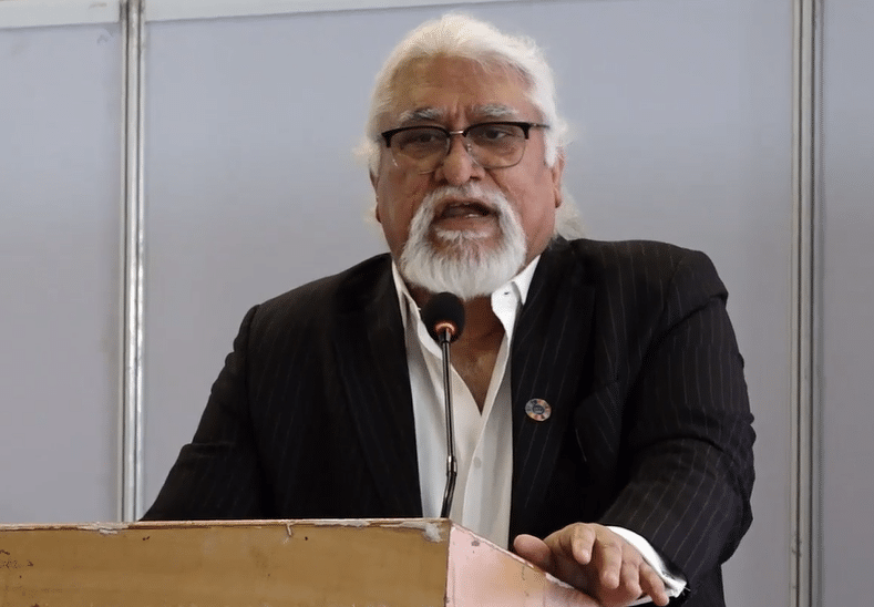
“We are at an inflection point. If we get our act together, ten years from now India will be a serious global player in semiconductor design and manufacturing.”
–Narang N. Kishor, Mentor and Principal Design Architect at Narnix Technolabs
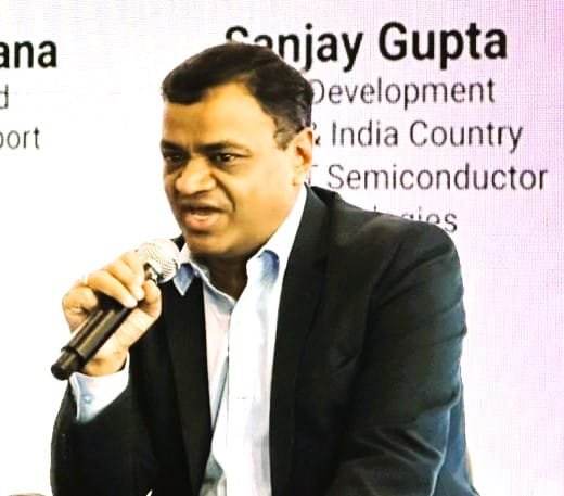
“Manufacturing scale is important, but real competitiveness comes when you control the architecture of the product and the key IP blocks inside it.”
–Sanjay Gupta, Chief Development Officer and India Country Head at L&T Semiconductor Technologies
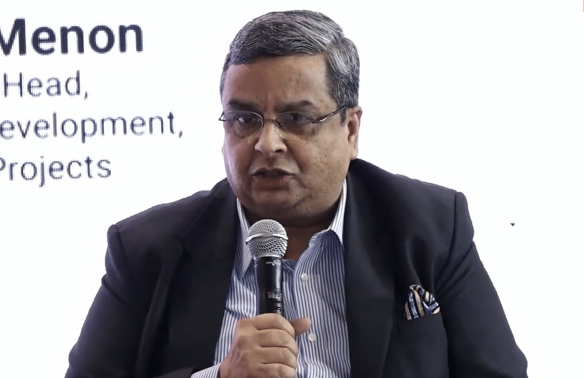
“We need to think in terms of conceived in India, designed in India, made in India, and used globally. That means solving real user problems. Consumers today expect global quality, like an iPhone.”
–PVG Menon, Vice President and Head of Business Development at Tata Projects
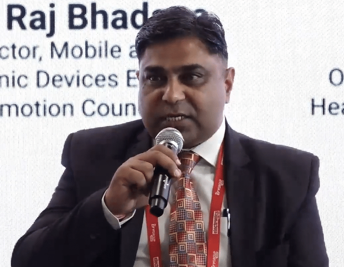
“From a neutral standpoint, one important shift is happening in how government approaches R&D funding.”
–Desh Raj Bhadana, Director at the Mobile and Electronic Devices Export Promotion Council
This article is based on the keynote panel discussion, ‘India’s ESDM Ecosystem: Charting the Path Towards Global Leadership,’ featuring Narang N. Kishor, Mentor and Principal Design Architect at Narnix Technolabs; Sanjay Gupta, Chief Development Officer and India Country Head at L&T Semiconductor Technologies; PVG Menon, Vice President and Head of Business Development at Tata Projects; and Desh Raj Bhadana, Director at the Mobile and Electronic Devices Export Promotion Council, held during EFY Expo Gujarat 2025. The discussion has been transcribed and curated by Shubha Mitra, Assistant Editor at EFY.