


Moving power lines to the back side of the wafer helps manage current flow in multi-stacked silicon. However, uneven thermal expansion between materials makes the wafer bend, affecting precision and yield.
As modern chips become smaller and faster, their internal design is changing to handle more power. Traditional chips send both signals and power through metal layers on the front side of the wafer. This setup works for older designs, but in advanced chips, it limits space and increases energy loss.
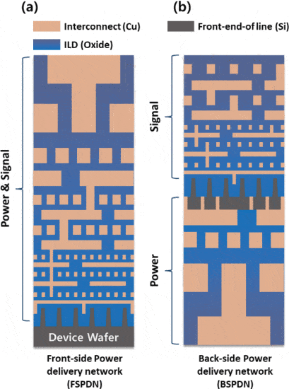
The backside of the wafer refers to the opposite surface of the silicon wafer from where the transistors and circuits are made. In new chip designs, this side is now used to route power lines, allowing electricity to reach transistors directly while freeing the front side for signal wiring.
Engineers are now shifting to a method called backside power delivery network (BSPDN), which routes power lines through the back of the wafer. The change improves electrical performance but introduces new mechanical challenges, primarily the bending of the wafer during production.
To find out why this happens, researchers from Korea published a journal article in IEEE Xplore, where they used computer-based simulations to study how stress builds up inside wafers during manufacturing. They examined key stages such as wafer bonding, thinning, and high-pressure heating.
The model shows that the wafer bends more as the process continues. The highest deformation occurs during heating at about 400°C, when materials inside the wafer, such as copper, silicon, and oxide, expand unevenly. This mismatch in expansion creates stress that causes the wafer to curve.
The study also explored how the amount of copper in the wafer affects bending. Changing the crystal direction of copper had little effect, but increasing copper density from 40% to 90% worsened the bending. The extra metal increased the difference in how layers reacted to heat, leading to more stress.
To limit this effect, the researchers recommend keeping copper layers balanced on both sides of the wafer and maintaining symmetry in the design. Adjusting the temperature and cooling rate during the high-pressure heating stage can also help. These process controls reduce stress and improve structural stability.
The findings give chip manufacturers a straightforward method to predict and manage warpage in BSPDN designs. This helps in producing thinner, more reliable chips as backside power networks become central to next-generation semiconductor technology.