


Engineers are developing ultra-thin analogue chips that can be stacked in 3D to deliver high performance in smaller semiconductor devices.
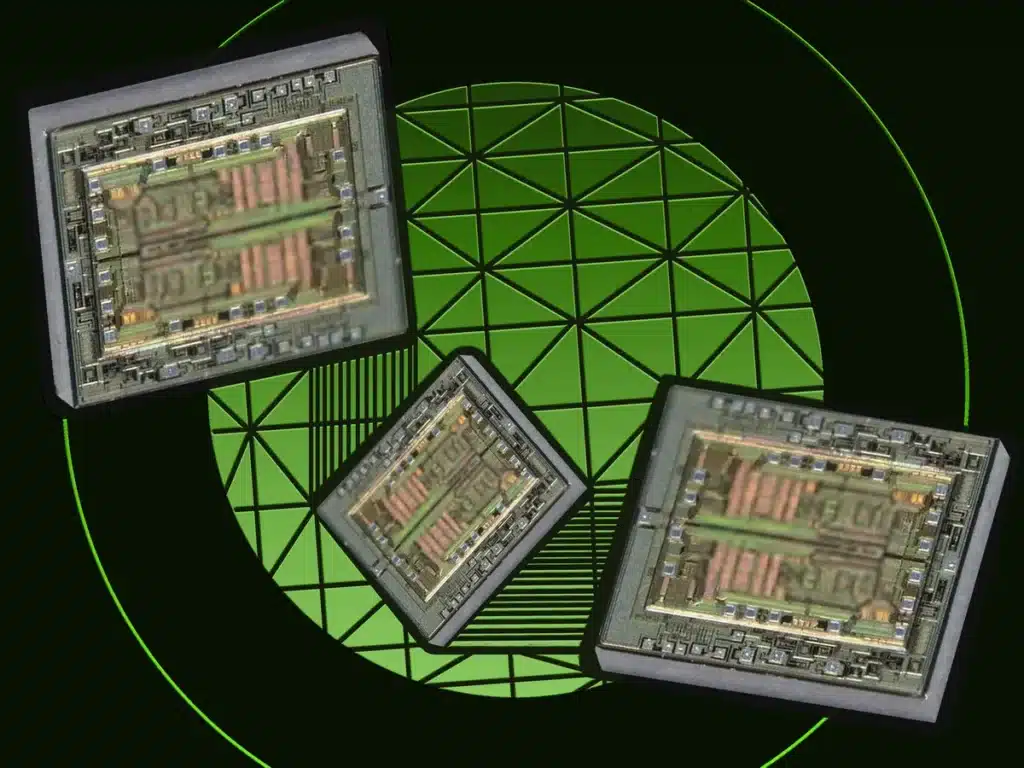
Oki Electric Industry and Nisshinbo Micro Devices in Tokyo are collaborating to develop a new type of thin-film 3D analogue IC. These chips are designed to make electronic devices smaller, faster, and cheaper to produce.

The new chips are made using Oki’s crystal film bonding (CFB) process. In this method, the top layer of a chip is lifted from its base and bonded to another thin chip layer using molecular forces. A thin insulation layer, such as silicon oxide, separates each chip layer.
The layers are connected using normal wire bonding. Because each layer is only 5 to 10 micrometres thick, the process can use standard, low-cost semiconductor tools instead of expensive advanced systems.
Stacking many thin analogue chips together creates a risk of electrical noise or “crosstalk” between layers. To fix this, Nisshinbo uses its own shielding method made from aluminium. The shielding is added only to areas that require protection to prevent unwanted electrical charge buildup. This helps keep the signals clean without affecting how the circuit works.
The companies are also applying this stacking method to chiplets. Small, modular chips that can be combined to perform different functions such as sensing, processing, or power control. This makes it easier to mix and match components, thereby improving manufacturing yield.
The companies are targeting the rising demand for analogue ICs used in AI systems, connected devices, and self-driving cars. These chips handle real-world signals like sound, light, and temperature and convert them into digital data for processing.
Both companies plan to bring this technology to market by 2026. They expect it will support the next generation of mixed-signal chips used in compact, high-performance systems combining analogue, digital, and optical components
