


A new laser-based manufacturing platform enables high-speed, high-precision metallisation directly on complex 3D parts, opening fresh design possibilities beyond flat PCBs.
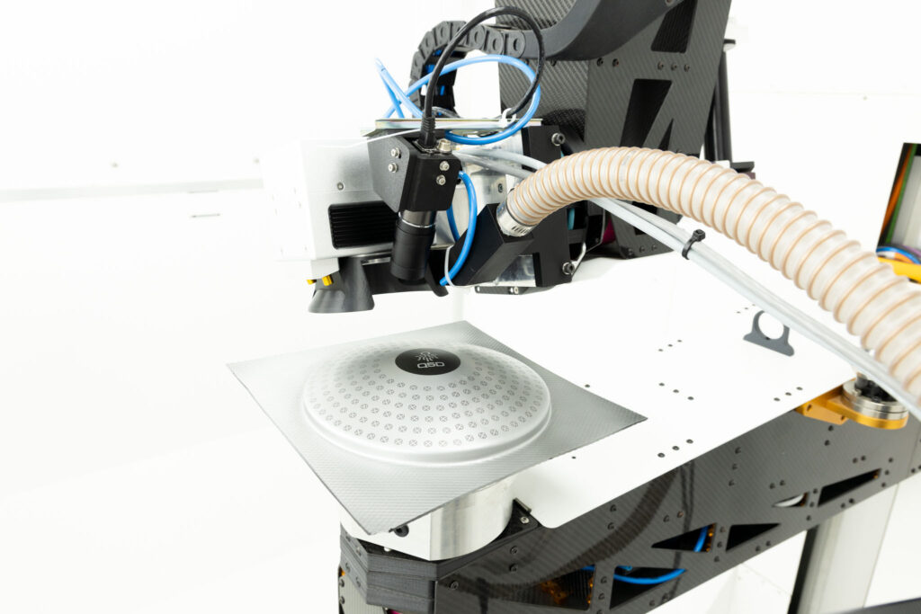
A newly launched five-axis laser metallisation system by Q5D is set to change how conductive circuits are created on complex three-dimensional components, especially in applications where traditional printed circuit boards fall short. The platform enables direct deposition of metal tracks onto large, contoured substrates, allowing electronics to be embedded seamlessly into product structures rather than added as separate assemblies.

The key features are:
- Five-axis robotic motion for true 3D circuit paths
- 100 W, 1064 nm laser for ablation and metal sintering
- Up to 1 m cylindrical build envelope for large components
- 150 µm line resolution with copper or silver deposition
- Fully digital CAD-to-part workflow with no retooling needed
Designed for precision electrification of 3D parts, the system uses a laser-assisted selective metallisation process to create conductive paths on polymers, ceramics, and specialised dielectric materials used in aerospace and high-performance electronics. This makes it suitable for manufacturing antennas, RF shielding, capacitive touch interfaces, sensors, and other functional electronics where geometry, weight, and integration are critical.
At the core of the platform is a five-axis robotic cell paired with a 100 W, 1064 nm laser head capable of both ablation and sintering. This combination allows circuitry to follow complex curves and surfaces with high accuracy, removing the design constraints imposed by flat substrates. With a cylindrical build envelope of up to one metre, the system is also geared toward large 3D components used in transportation, aerospace, and industrial equipment.
The process supports fine-feature deposition, achieving line resolutions of around 150 microns using copper or silver, with metal layer thicknesses ranging from 1 to 15 microns depending on application needs. A fully digital workflow, from CAD design to finished part, significantly shortens development cycles and enables fast changeovers without mechanical retooling—an advantage for both prototyping and low-to-medium volume production.
Beyond precision and speed, the system introduces a shift in design philosophy. By integrating conductive features directly into structural parts, manufacturers can reduce part count, wiring complexity, size, and weight while improving reliability. The machine can operate as a standalone unit or be integrated into existing production lines, supporting scalable adoption across industries.
