What happens when electronic parts become hard to see? A new method shows how engineers can fit more functions onto the same circuit board.
There is a growing shift toward edge AI, where data processing happens directly on the device. At the same time, everyday products such as smartphones, wearables, and medical devices are starting to analyze information on their own. As these devices become more advanced, the number of electronic parts used on each circuit board is rising. This makes further miniaturization and higher-density component placement essential.

Fuji Corporation, based in Chiryu, Aichi, announced that it has achieved the world’s first successful placement of 016008 mm size electronic components on printed circuit boards using its NXTR SMT pick-and-place machine. This was made possible by newly developed machine technology designed to handle next-generation ultra-small components. The demonstration was presented at the 40th NEPCON JAPAN Electronics R&D and Manufacturing Technology Expo held on January 21, 2026, at Tokyo Big Sight. According to Fuji’s research as of January 15, 2026, this is the first achievement of its kind.
Fuji has developed fast and accurate pick-and-place machines that can reliably handle very small components, and recent advances in four key control technologies have made it possible, for the first time, to place 016008 mm (006003″) size components on PCBs by checking component orientation and position in real time, correcting pickup errors and static effects for stable pickup, precisely controlling placement force to avoid damage, and using nano-level position correction to achieve extremely high placement accuracy.
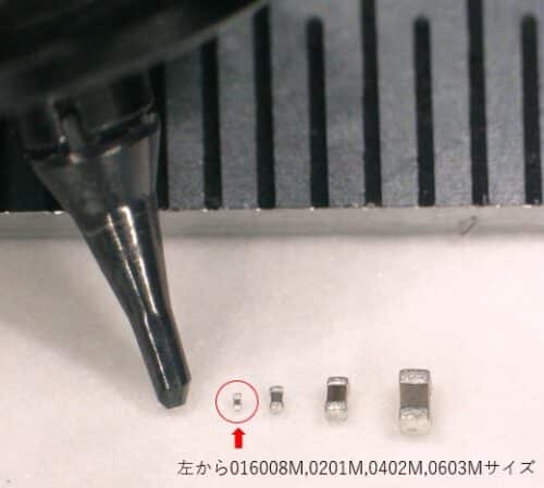
The 0201 mm component size, long considered the smallest standard in mass production, is now reaching its practical limits. To support higher circuit density, a new component size, 016008 mm, is being developed. These components need about half the mounting area of 0201 mm parts, allowing more functions to be packed into the same board space.

To place components of 016008 mm (006003″) or smaller, it is necessary to improve not only the placement step but also all related steps, including panel design, solder paste, stencils, reflow, and inspection. Fuji is advancing placement machine technology and working closely with partners to build a complete process solution that covers equipment and materials, helping push electronic component miniaturization to the next level as the edge AI era begins.