


In today’s digital landscape, seamless connectivity and communication are essential for the smooth operation of various electronic devices. The USB to Serial TTL Converter with a USB Type-C connector represents a pivotal solution in bridging the gap between modern USB interfaces and traditional TTL-level circuits.
As USB Type-C connectors continue to gain widespread adoption due to their versatility and compact design, the need for compatible communication interfaces becomes increasingly vital. This project addresses this demand by offering a reliable and efficient converter that enables bidirectional data transfer between USB-enabled devices and TTL level circuits.
The USB to Serial TTL Converter provides a flexible and user-friendly interface, allowing developers and enthusiasts to interface with a wide range of TTL-level components, such as microcontrollers, sensors, and other embedded systems. Its integration of the USB Type-C connector ensures compatibility with the latest generation of devices while offering enhanced durability and ease of use.
This project not only simplifies the process of serial communication but also opens up possibilities for diverse applications, including prototyping, debugging, and data logging. Whether for educational purposes or professional development, the USB to Serial TTL Converter serves as a versatile tool for electronics enthusiasts and engineers alike.
Component Required
- Capacitor
- LED’s
- ESD Protection diode
- USB Type C connector
- Resistor
- Inductor
- Right-angle male header
- USB to serial TTL IC
Bill of Materials
| Item | Qty | Reference(s) | Value | Per unit price in INR | Price as per quantity in INR |
| 1 | 2 | C1, C3 | 4.7uF | 2.4 | 4.8 |
| 2 | 4 | C2, C4, C5, C6 | 100nF | 1.37 | 5.48 |
| 3 | 2 | D1, D4 | SM712_SOT23 | 17.59 | 35.18 |
| 4 | 2 | D2, D3 | LED-SMD-RED DIFFUSED_0603_ | 2.51 | 5.02 |
| 5 | 1 | D5 | 5988A80107F | 22.6 | 22.6 |
| 6 | 4 | H1, H2, H3, H4 | Mounting Hole_Pad | 0 | 0 |
| 7 | 1 | J1 | USB4105GFA120 | 18.9 | 18.9 |
| 8 | 1 | J2 | 61201021721 | 9.56 | 9.56 |
| 9 | 1 | L1 | 120R | 1.19 | 1.19 |
| 10 | 4 | R1, R2, R3, R4 | 1K | 0.39 | 1.56 |
| 11 | 2 | R5, R6 | 5.1K | 0.39 | 0.78 |
| 12 | 1 | U2 | CP2102N-Axx-xQFN20 | 200 | 200 |
| Total | 305.07 |
Schematic
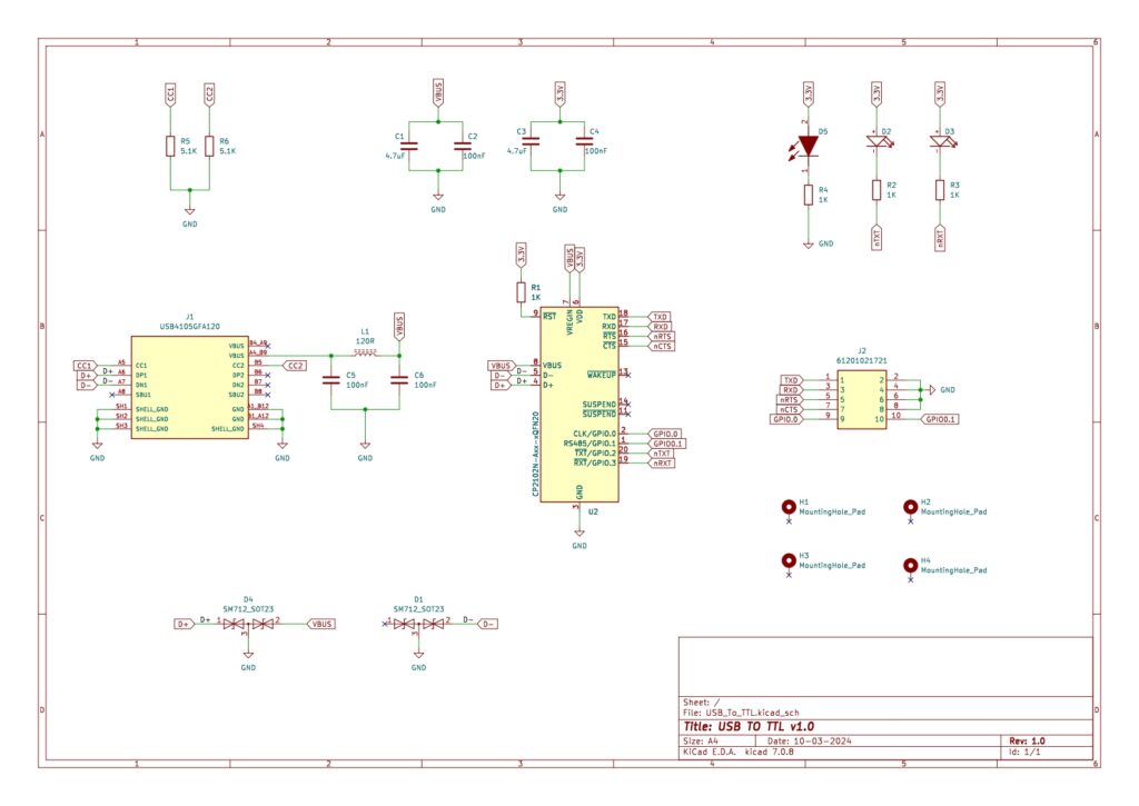
Download Schematic PDF
Hardware Design
1. Software Used:
The project harnesses the capabilities of KiCad (7.0.8), an open-source Electronic Design Automation (EDA) software suite renowned for its robust features and user-friendly interface. KiCad facilitates seamless schematic capture, PCB layout, and 3D modeling, making it an ideal platform for designing complex electronic systems.
2. PCB Dimensions:
The physical dimensions of the PCB are engineered to meet the requirements of the project, ensuring compatibility with standard enclosures and integration into various electronic systems.
With a length of 40.38mm and a width of 22.66mm, the compact form factor of the PCB maximises versatility while minimising footprint.
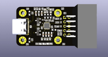
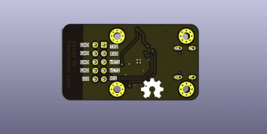
3. PCB Layers:
The PCB is crafted with 2 layers, carefully optimised to balance signal integrity, routing efficiency, and manufacturability.
The top layer serves as the primary routing layer, accommodating signal traces and component placement. Meanwhile, the bottom layer is utilised for additional routing and establishing a solid ground plane, crucial for minimising noise and enhancing signal integrity.
4. ESD Protection Diodes:
ESD (Electrostatic Discharge) poses a significant threat to electronic devices, especially those with exposed connectors like USB Type-C.
To mitigate this risk, the hardware design incorporates ESD protection diodes.
These diodes act as a first line of defense, shunting potentially harmful electrostatic discharge away from sensitive circuitry. By providing a low impedance path to ground during ESD events, they safeguard the USB Type-C connector and associated components from damage or malfunction.
5. Differential Routing and Length Matching:
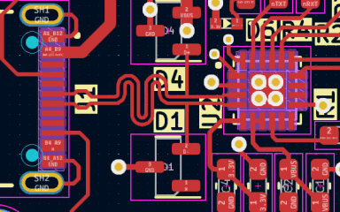
Differential signalling is paramount for high-speed data interfaces like USB Type-C, where accurate signal transmission and reception are critical for reliable communication.
Differential pairs are meticulously routed with attention to length matching, ensuring that signals arrive at their destination simultaneously and reducing the risk of skew.
This meticulous approach enhances signal integrity and minimises electromagnetic interference (EMI), guaranteeing robust performance in demanding environments.
6. CP2102N IC Integration:
The design features the integration of the CP2102N USB to UART bridge controller, a highly versatile and widely used IC renowned for its robust performance and feature-rich capabilities.
The CP2102N not only facilitates seamless USB to UART conversion but also offers GPIO (General Purpose Input/Output) pins that can be configured for various purposes, including TX (transmit) and RX (receive) indication functionalities.
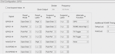
With the flexibility to configure GPIO settings using Silicon Labs’ Simplicity Studio software suite, developers can tailor the functionality of the CP2102N to suit specific application requirements, enhancing versatility and customization options.
7. PCB Fabrication:
Leveraging local expertise and resources, the PCB is fabricated in India by PCB Power, tapping into the country’s burgeoning electronics manufacturing sector.
Local fabrication offers numerous advantages, including shorter lead times, cost-effectiveness, and the ability to collaborate closely with manufacturers to fine-tune production processes and ensure high-quality results.