
New bidirectional GaN switches reduce PCB space requirements, lower power losses, and improve efficiency for smartphones, notebooks, and wearable electronics.
Portable consumer electronics continue to face increasing pressure to deliver more performance within smaller form factors. Addressing this challenge, a new generation of gallium nitride (GaN)-based bidirectional power switches has been introduced to reduce component count and board space while improving power efficiency in compact devices.

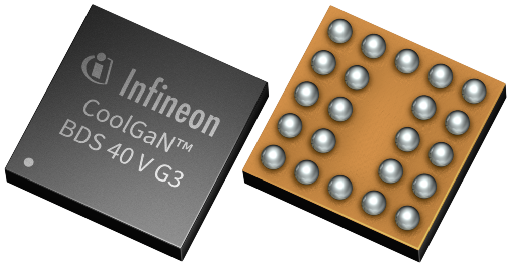
Infineon Technologies AG’s latest additions to the power switch portfolio target smartphones, notebooks, and wearable products where PCB real estate is increasingly constrained. By integrating the functionality of two back-to-back silicon MOSFETs into a single component, the new devices reduce component count by half and shrink PCB footprint requirements by up to 82%.
The integration approach allows designers to simplify board layouts without major changes to existing power architectures. Since the devices support standard 5 V gate drive operation, engineers can reuse current driver layouts, potentially shortening development cycles and minimizing redesign efforts.
The key features are:
- Up to 82% PCB footprint reduction
- Reduces component count by 50%
- Up to 40% lower gate charge
- More than 85% lower leakage current
- True bidirectional voltage and current blocking capability
Packaged in wafer-level chip-scale packages measuring 2.1 × 2.1 mm² and 1.7 × 1.2 mm², the devices are optimized for high-density designs. The larger variant delivers an on-resistance of 4.2 mΩ, while the smaller version achieves 9 mΩ, enabling lower conduction losses in portable power systems.
The devices also introduce performance improvements associated with GaN technology. Gate charge is approximately 40% lower than comparable competing solutions, enabling faster switching speeds and reduced switching losses in applications such as fast charging systems. Lower switching losses can help improve overall power efficiency while reducing heat generation.
Leakage performance has also been enhanced, with drain-to-drain leakage current reduced by more than 85% compared with competing alternatives. Reduced leakage and thermal stress can improve long-term reliability and support stricter safety requirements in compact electronics.
Unlike conventional silicon MOSFET designs that depend on body diodes and may permit unintended reverse current flow, the new devices provide true bidirectional voltage and current blocking capability. This feature is particularly relevant in USB overvoltage protection systems, load switching circuits, and power multiplexing applications where current direction control is critical.
The expanded family is designed to cover a range of mobile power switching requirements, from space-constrained wearable devices to higher-performance notebook systems.
Click here for the original announcement.