


New advances in electronic-photonic integration aim to deliver faster, more energy-efficient communications while reducing the environmental impact of data transmission.
The MIT-led FUTUR-IC research project has made several significant advances in electronic-photonic integration that will allow future communication devices to have high bandwidth and higher efficiency. This program intends to make microsystems that can transmit information in excess of 1 petabit per second.

This system is a combination of electronics and photonics because electronics handle data processing through electricity, whereas photonics transmit the data through light. According to researchers, these microsystems can also be fabricated using existing electronics foundries and packaging infrastructure. Advanced systems using co-packaged optics can provide improved bandwidth and energy savings compared to the current electronics-based and pluggable optical systems.
“Our disruptive electronic-photonic integrated solutions will enable us to leap from [transmitting data at] hundreds of terabits per second to greater than 1 petabit per second,” said Anu Agarwal, who leads MIT’s FUTUR-IC, at an April webinar titled “Shaping the Future of Semiconductors: Power, Performance, and Possibility.”
They observed that there is a rapid growth in the number of data centres, which may use almost 10% of the world’s electricity by 2030. In addition to that, they pointed out that the microchips were responsible for about 500 megatons of carbon dioxide equivalent lifetime emission in 2021, whereas every year the world produces more than 50 million tons of electronic waste. The merging of photonics and electronics can play a significant role in overcoming such environmental problems, as data transmission via light is comparatively more energy-efficient.
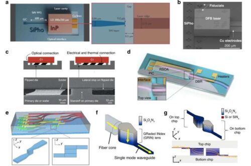
FUTUR-IC has successfully created three optical couplers, making it easier and less expensive to integrate photonic chips with microchips. The evanescent coupler appeared on the cover of Advanced Engineering Materials, whereas the graded index coupler (GRIN) was reported in the March 2026 issue of Journal of Physics: Photonics. A third coupler developed by MIT researchers led by Juejun Hu was reported in Laser & Photonics Reviews in 2023. These three couplers are the first optical equivalents of solder bumps utilized for chip-to-chip and chip-to-substrate connections.
Aside from developing new hardware, the programme has created Earthster, a visualization model that will enable companies to quickly determine the energy use, materials usage and environmental sustainability across a company’s products. Additionally, the programme has established various educational activities such as a MOOC on the efficient use of semiconductors’ resources, gamification of digital learning, a summer academy, a bootcamp and TED-Ed videos for K-12 awareness.