





Can PCB fabrication keep pace with shrinking circuit geometries? A manufacturing upgrade is aiming to improve precision for increasingly dense board designs.
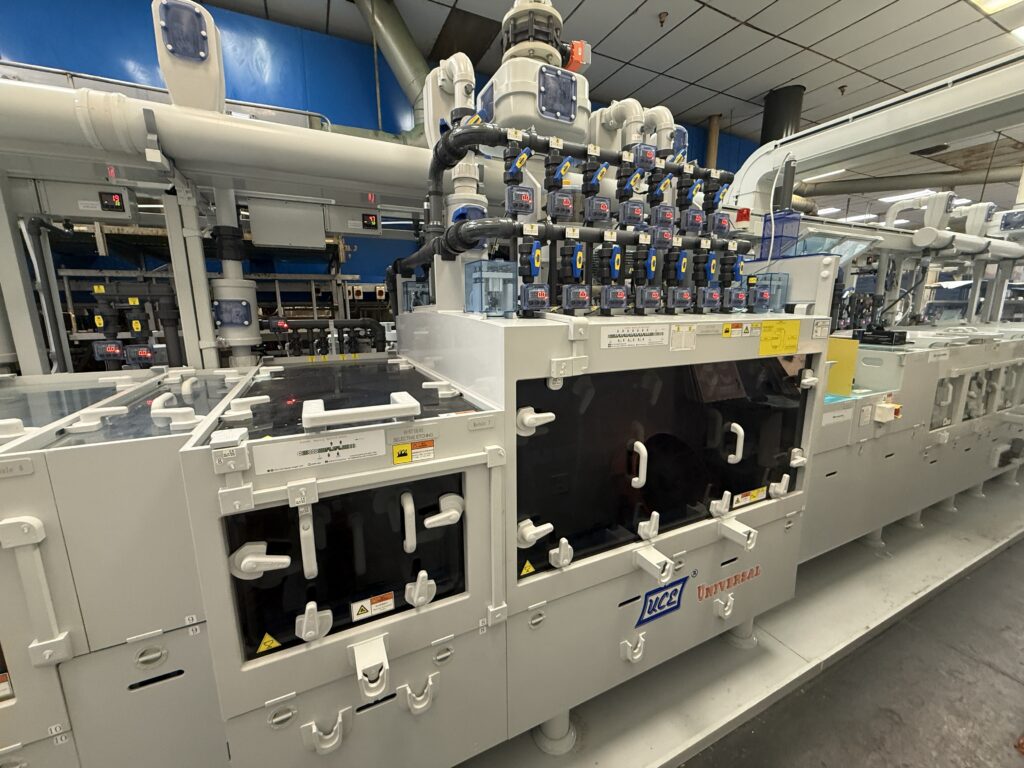
AdvancedPCB has installed a new Strip-Etch-Strip (SES) wet-process line at its manufacturing facility in Aurora, Colorado, as part of its 2026 Technology Acceleration Initiative. The upgrade is intended to strengthen the company’s PCB manufacturing capabilities and support the production of advanced printed circuit boards with finer features and higher layer counts.
The SES process is a critical stage in PCB inner-layer fabrication, where copper circuitry is patterned before individual layers are laminated together. Maintaining precise control during this step is essential for achieving accurate line widths, spacing and layer registration, all of which directly influence board quality and manufacturability. As electronics continue to demand denser layouts and tighter tolerances, improvements in inner-layer processing become increasingly important for reliable production.
Supplied by Equip Tech and manufactured by Universal Circuit Board Equipment Co. (UCE), the new production line integrates automated chemical management, conveyorised material handling and process controls throughout the strip, etch and strip cycle. The system is designed to support a wide range of PCB technologies, including high-density interconnect (HDI), multilayer and other high-density circuit board designs.
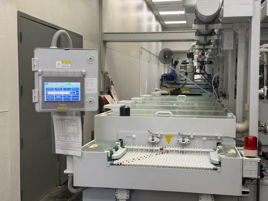
The installation was completed during a scheduled production shutdown over the US Independence Day holiday weekend to minimise disruption to customer manufacturing schedules. The Aurora facility focuses on quick-turn PCB fabrication and prototype assembly, supporting customers from product development through low- to mid-volume production.
“PCB designs continue to become more complex, and it’s our responsibility to invest ahead of our customers’ needs,” says Greg Halvorson, Chief Executive Officer at AdvancedPCB. “The SES line is one of several manufacturing investments we’re making throughout 2026 to ensure our facilities are equipped to support the next generation of electronics while delivering the quality, responsiveness, and manufacturing expertise our customers depend on.”

