

A new photonics platform aims to simplify chip development, combining optical components and design tools to support faster, higher-capacity data centre connections and sensing.
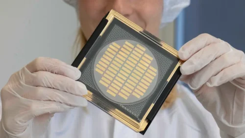
OpenLight and Tower Semiconductor have expanded their photonics ecosystem through the PH18DA Photonics process design kit (PDK), making the platform available through Cadence electronic design automation tools. The development is intended to accelerate high-performance photonic chip development for data centres and other advanced optical systems.
The platform allows active photonic components, including lasers, modulators and amplifiers, to be integrated into a single monolithic photonic chip. By bringing these elements together within an established design environment, the approach could make photonic integrated circuit development more similar to conventional electronic integrated circuit design.
According to the companies, the expanded ecosystem combines photonics technology with chip manufacturing expertise and electronic design tools. Making the PDK available through established design software is intended to help engineers create integrated photonic circuits within the same environment used for advanced IC development.
The technology is aimed particularly at optical communications and high-performance data centre infrastructure. As demand for computing and data processing continues to increase, optical connections can provide a route towards higher bandwidth and improved efficiency.

The platform is also designed to support advanced near-packaged optics and co-packaged optics. These approaches can bring optical functions closer to electronic processing components, potentially helping to address performance, power and scalability requirements in next-generation systems.
The companies are targeting 400G and 1.6T laser-integrated photonic circuits. Such capabilities could support the development of optical systems designed for increasingly demanding data centre applications.
The collaboration also brings manufacturing and design capabilities together, providing a more integrated route from photonic design towards production. The companies say this could help streamline development of high-performance optical systems while improving design efficiency.
Beyond data centres, the underlying technology could potentially support optical connections, smart systems and sensing applications. The development therefore represents a broader effort to make advanced photonic integration more accessible through established semiconductor design and manufacturing workflows.