Flash memories have been around for a decade in all sorts of embedded systems. These are used both as code space and non-volatile memory to save data across power cycles.
As we utilise flash to store the configuration data and history records, it is important to predict the lifespan of the product and the number of saves to flash per day in the emerging consumer electronics applications. Though many devices claim a higher number of write cycles, they may be hard-pressed to meet the operating conditions.

Another important concern is the time to write and erase on a memory block. Allen Pothoof, senior software engineer from Esterline Avista, shares, “Erase/write time is important because if you haven’t planned for it, your application may come to a screeching halt while you update some data.”
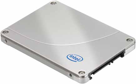
Flash memory vendors are competing against each other not on process-technology but application-specific solutions to meet the demand coming from emerging consumer applications like tablet PCs, mobile phones, solid-state storage devices, audio players and television sets with digital recording function. for all these devices, to make full use of the benefits offered by flash memories, it is necessary to understand how to rewrite on them.
Flash penetration in embedded apps
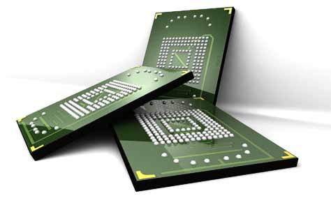
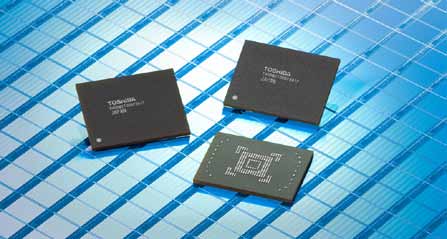
There are different types of flash memories available in the market. The type of embedded application determines the type of flash memory that needs to be utilised—while some flash memory companies may be targetting the data storage flash used in applications like SSDs and memory cards, others target a different type of flash used in applications like smart meters, networking equipment, DVD players and Bluetooth products in addition to smartphones and tablet PCs.
Leonid Rosenboim, embedded systems entrepreneur and founder of Certarete, informs, “Initially, flash was used as a replacement for the ultraviolet erasable programmable read-only memory (UV EPROM), mainly to store the program code and data. Some systems used the EPROM/flash in ‘execute in place’ mode to save the RAM, while others copied the code to the RAM to gain a higher execution speed.”
Gradually, “flash grew to replace the electrically erasable programmable read-only memory (EEPROM) by utilising its ability to be modified ‘in-circuit’ and store non-volatile modified ata (such as configuration). Later, more sophisticated embedded systems deployed one of several file system technologies (either fast file system or flash transition layer) to store larger portions of data and program code that was easier to modify (upgrade) in these file systems,” says Rosenboim.
More recently, the file system portion has been increasingly taking advantage of the cost-effective NAND technology. NAND is being used for data storage in addition to OS/apps storage for the applications processor. Richard De Caro, director of strategic marketing for Atmel’s memory business unit, says, “In these cases, portions of the NAND flash are shadowed into the DRAM and the code executed out of the DRAM and not the NAND flash. Standard NAND flash does not provide fast random-access read that is needed for code execution. However, NOR flash is still used in most mobile phone designs as the code-execution flash for the baseband processor.”
Open NAND Flash Interface (ONFI) Working Group
The Open NAND Flash Interface is an industry working group made up of more than 80 companies that build, design-in or enable NAND flash memory. The group is dedicated to simplifying NAND flash integration into consumer electronics products, computing platforms and any other application that requires solidstate mass storage. They define standardised component-level interface specifications as well as connector and module form factor specifications for NAND flash.
The ONFI Working Group was formed in May 2006 and currently has more than a hundred member companies. ONFI’s founding companies include Hynix Semiconductor, Intel, Micron, Phison, SanDisk, Sony and Spanion.
Another interesting trend is that many microcontrollers and even some field-programmable arrays (FPGAs) are now made with embedded flash memory to decrease the component count and cost of embedded systems. All the microcontrollers use an internal, on-chip flash memory for data storage. Embedded flash platforms are also being used for programmable device and systems-on-chip development.
Richard also notes, “while many microcontroller solutions have embedded flash, the memory density in many cases is not large enough to store the entire system firmware, especially as application feature sets increase and user interfaces become more interactive and sophisticated. Therefore systems will still incorporate an external flash solution for direct code execution or for code shadowing.”
Write/erase speed on flash memories
Writing to flash memories is a slow process. Harry Kitt, R&D technical associate, Spacelabs Healthcare, shares, “when the system needs to store substantial data, the real-time element is suspended for the system’s first purpose. when you are considering the dump-truck-sized flash chip, keep in mind that the only way to fill it is wit a teaspoon.”
Explaining how the write/erase operation works, Rosenboim says, “Typically, the write speed of flash memories is of the order of a few microseconds per byte, but a write operation will only change bits from ‘1’ to ‘0’. So to write arbitrary data, an entire ‘block’ must be erased first, which will turn all bits to ‘1’.”
It is a major limitation of flash memories that these can read or program a byte or a word at a time, but can be erased only in blocks. So the rewrite and erase operations are not in random-access fashion. An erase operation takes 0.1 to 5 seconds, depending on the specific technology, and typically erases 64 to 128 kB at a time.
Some vendors offer a type of flash memory that helps alleviate the drawback of spending hundreds or thousands of milliseconds to erase large blocks of memory by allowing the system to erase very small pages of memory. Explaining further, Richard says, “You can erase as little as 256 bytes of memory at a time, and the erase typically takes less than 15 milliseconds. This kind of erase granularity provides the added benefit of not forcing the system to erase more memory than is actually needed for a particular operation, which allows the system to optimise the memory array usage and the system performance.”
Flash components primarily come with either of three interface types: Parallel, byte-serial and bit-serial. Rosenboim says, “Since the NOR flash has traditionally been used to replace the EPROM and ‘eXecute In Place’ the code, it has a parallel address/data interface that is ‘memory mapped’ onto any type of processor by directly interfacing its local bus signals.”
Today, the price of the NOR flash has come down to a point where its package is the most significant component of the cost. To reduce the cost further, a reduction in the number of pins on the package resulted in introduction of ‘bit-serial’ interface components like serial peripheral interface (SPI) based flash. These parts require a special module in the microprocessor to initialise its DRAM controller and copy the entire boot code section into the DRAM for execution.
“Typically, NAND flash components come with a byte-serial interface, where a command byte and a few address bytes are followed by a whole ‘page’ worth of data bytes on the same 8-bit data interface. That is, the bytes are serially transmitted between the flash device and the microprocessor,” shares Rosenboim.
“The more recent NOR flash based devices—those with multi-level cells—have become much slower to erase than their predecessors. four seconds to erase a 128k block is truly slow by any measure, but it appears these are made necessary by the changes in technology that lead to lower cost per bit and higher densities,” he adds.
On the positive side, these newer NOR parts have an improved erase-suspend ability. So with a bit more complexity of the software layer, one can mitigate this problem by suspending the erase process to let other activities execute while performing the erase operations in the background effectively. This is much less of a problem than all operations being blocked for the duration of a ‘block erase’ operation.
If the application requires a lot of inputs/outputs (I/Os) for booting, one may opt for industrial-grade flash devices that can handle the demanding speed.
Endurance: how many times can you rewrite/erase?
The critical use of flash memories in consumer products like MP3 players, USB pen drives and digital storage TV sets is to rewrite the information onto the memory. what comes into consideration here is the limitation of finite program/erase cycles.
Like any other erasable memory, flash devices have a limited number of erase/write cycles that they can withstand without failure. The reason for the limitation depends on either the charge-trapping characteristics or the dielectric-breakdown characteristics of the tunnel oxide. This introduces a term called ‘endurance.’
Brian Beckham, manager-software design, Lester Electrical, says, “while using flash devices, we need to ensure that we stay below 50k writes within the expected product life.” Though many devices claim a higher number of cycles, typically 100k, it is better to design within the life expectancy of the flash device than to try and extend it, he feels.
There is no guarantee to how long the parts or blocks will work. As long as the memory is used to store the pro-gram code, it is very unlikely that the application will reach the maximum guaranteed erase cycles. If you really think of it—how many times do you upload a new design code for the application? But when using the flash for data storage, the entire game changes. So the designers must carefully calculate the worst-case scenario.
Let us take the example of a consumer electronics device that stores configuration settings with each power-down cycle. Only the change in the setting is stored to optimise the code.
If we assume that it uses two 16k flash sectors and the configuration data occupies 32 bytes, a total of 10,000 entries can be made before both the sectors go through an erase cycle. So a hundred million writes can be made before the system reaches the maximum number of erase cycles.
You can do the basic maths to calculate the maximum number of writes in a day for the device to last up to ten years.
“You can also implement a battery back-up cache RAM section to decrease the write cycles to the flash memory,” suggests David Quinn, a hardware design and firmware engineer, QED.
Design considerations
flash memories are making inroads into almost every consumer application either for code storage or for data storage. Depending on the type of the application, there are several aspects that need to be considered while using flash in an embedded application design.
Understanding the write/erase cycles will help you design the product for life expectancy. But sometimes harsh environments may limit the life-time of the products by affecting their components.
The embedded designer should be aware of the page size as well as erase/write time. Pothoof says, “The page size, along with data layout, is important because you don’t want to erase a 1k page to update a single byte.” The designer should also pay attention to the kind of power plan present while doing the updates. “Having a user pull the battery when you are in the middle of an erase cycle can lead to some very interesting and hard to fin errors,” explains Pothloof.
Temperature is another important consideration. The flash drive—the most stable device in optimal conditions—shows erratic behaviour at extremely high or low temperatures. Issues like corrupt data, slow response time and system error can occur.
“we also use write verification code with checksums, trap all errors from the device and apply other methods to ensure proper operation. flash is a useful and inexpensive device but like all the hardware deployed within embedded systems, the life, error trapping and temperature ranges must be paid attention to,” shares Beckham.
Sharing interesting observations on a project on emulating the EEPROM inside the flash memory to store specific data before shut-down, Nistor flavin, a hardware developer from Continental, says, “first of all, if you have a cache memory, you can’t use it any more or you have to use the memory management unit (MMU) settings to make that area non-cacheable. The read time is small compared to the erase time.”
He explains, “for this, you have to use two memory blocks—one active and the other blank—in order not to erase a block every time you want to update a byte (you will need to erase the block only when it is full). If the software is done in a good way (keeping track of all steps), even if you shut down the system during an erase operation, no problem should appear.”
The road ahead
The flash memory has been the work-horse of embedded systems. However, device manufacturers have been on a constant endeavour to eliminate its major drawbacks like block-only erasability, slow erase times and limited erase/write cycles (which limits its life as a data storage device).
Flash Memory Vendors
• Samsung
• Toshiba
• Hynix
• Atmel
• Intel
• Micron
• Numonyx
• PowerChip
• Spanion
• Macronix International
Ashish Gupta, R&D group leader, The Learning Labs, says, “One such technology which addresses these concerns is the phase-change memory (PCM). It works by taking advantage of the alter-able physical and electrical properties of certain materials in order to store information on a memory device.”
PCMs are being designed to keep the hardware interface (both in the case of SPI based and parallel data bus based devices) similar to the traditional flash memory devices. The software interface (command codes for performing various functions like program, erase and read the device ID) is being designed to be very similar to existing flash memories. Hence migration of existing designs is easier.
Gupta claims, “These may or may not be at the right price point yet, but surely the future seems bright.”
PCM-based devices are already available in the market. Listing the benefits of the PCM technology, Gupta says, “Bit alterability, which is the ability to change each memory bit independently from 0 to 1, or 1 to 0, without an intervening ‘block erase’ operation, significantly reduces software overheads.”
This technology offers a higher endurance. That is, an increased number of write cycles (of the order of 1,000,000, as claimed in the datasheet) reduces the need for wear-levelling algorithms employed in flash file systems like the journaling flash file system. It has faster access speeds that offer faster erase cycles and faster write cycles. Also, no sector-erase is needed for programming.
To conclude
Flash memories have proven their benefits in both code storage and data storage. However, like any other semi-conductor device which is programmable and erasable, it is important to understand their physical parameters. for data retention, data integrity, endurance and reliability of the application, the datasheets and design specification must be studied carefully. Verification codes and other software codes can be used to check the flash contents.
Today, on-chip flash has replaced the EEPROM in applications that need to store configuration data during power-down and power-up cycles. Looking forward, memory vendors are trying to commercialise a next-generation technology that can combine DRAM and NAND together.
The author is a senior technology journalist at EFY