Many electrical and optoelectronic devices need metal-semiconductor junctions. It can be challenging to make high-quality junctions that integrate traditional metals with 2D semiconductors, despite the fact that they are now produced and used on a global scale.

A novel technique has recently been created by scientists at the Chinese Academy of Sciences, Hunan University, City University of Hong Kong, and Fudan University. This technique may be used to more efficiently transfer metal electrodes on 2D materials, allowing for the development of more dependable metal-semiconductor junctions. This method was described in a publication that appeared in Nature Electronics. It involves delaminating metal electrode arrays from a graphene wafer and then printing them onto various 2D substrates.
“For the first time, in 2013, we reported that continuous graphene monolayers can be grown via CVD directly on semiconducting Ge(001) surfaces, making a significant departure from conventional metallic systems,” Zengfeng Di, one of the researchers who carried out the study, told TechXplore. “Because of the insulating property of intrinsic Ge at the temperature below 10K, we carried out the research on graphene-mediated superconductivity in the metal nano-islands/graphene hybrid on Ge substrate, without the transfer of graphene from Ge substrate to SiO2 substrate.”
Di and his colleagues discovered during their earlier research that metals put on graphene may be pulled off quite readily. This was also true for metals like titanium or nickel, which are notoriously hard to peel off of silica substrates.
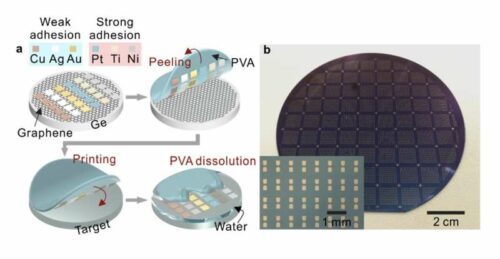
The team’s method was applied in their most recent investigation to deposit six different metal types onto a wafer-scale graphene/Ge donor substrate. This comprised both strongly adhering metals, such as platinum, titanium, and nickel, as well as weakly adhering metals, such as copper, silver, and gold.
There are multiple steps in the researchers’ method for integrating metal electrodes on 2D materials. A metal electrode array must first be deposited on a graphene/Ge substrate. A polymer film can be used to easily peel the array away from the surface of the substrate because graphene has no dangling connections.
“After removing the polymer film by deionized water, wafer-scale 3D metal patterns can transfer onto an arbitrary target,” Di said. “Compared with the previous transfer printing methods using silica substrate, we can transfer arbitrary metal with 100% yield and scale up the transfer technology to wafer size.”
“Beyond a simple 2D transistor, we are using this technique to fabricate basic 2D logical units, including AND-OR, NOR, and AND gate,” Di added. “In addition, the cost of our approach should be further reduced by optimizing the process and increasing the reusability of graphene/Ge substrate.”


