


In the world of electronics goods, where margins are razor thin, manufacturers try to keep product cost low to maintain a competitive edge. In a bid to achieve this, they tend to constrain designers to achieve the desired function by using lowest-cost PCBs and circuit components. Using electromagnetic compatibility (EMC) design techniques for PCBs and selecting components with high levels of EMC is a luxury, they think, they cannot afford.
Most are of the opinion that problems can be fixed using additional EMC suppression components (aptly called electromagnetic interference or EMI fixes) at the end of the product development cycle, if at all it is found that these are really required. Following this approach, it is not immediately obvious that the cost of these last-minute fixes will in fact be many times the cost of EMC measures incorporated during PCB design in the initial stages of the product development cycle. So the approach of lowest bill of material cost will actually result in considerable increase in product cost.
In order to design a PCB with low emission and susceptibility, two aspects have to be kept in mind. First, the ground (or signal return) system and second the PCB layout. For any PCB it is desirable to have a low-impedance ground system that is effective in draining out EMI currents, but it is the PCB layout that is the single-most-effective factor in designing a good PCB; a good layout not only reduces ground track impedance but also avoids common impedance coupling.

High speed PCB design: Digital circuit layout and noise
Digital ICs incorporating logic gates are often a source of impulsive transients due to finite charge recovery times of transistors. Whenever a logic gate changes state, a short pulse of current is drawn from power supply rails because both the totem-pole transistors at the output momentarily conduct. Now the inductance of ground tracks opposes this sudden change producing a back electromagnetic force, which shows up as a spike. This spike is referred to as ground bounce or shoot-through.
In order to reduce this generated transient, all such circuits must be designed with a low-inductance ground system. Also, a source of charge should be provided near each logic gate, which ensures that the high transient current is not drawn all the way from the Vcc.

The ground track impedance can be reduced by reducing the value of track inductance, reducing the loop area enclosed by the current spike and by reducing the length of the tracks over which this current flows by providing a source of charge near each logic gate.
Reduction of ground track inductance
The inductance of a PCB trace is directly proportional to its length. This can be used to advantage by minimising the length of critical traces that carry this high transient current. A further reduction can be achieved by increasing the width of the power supply traces.
However, the inductance of a track is inversely proportional to the log of track width. Hence it is difficult to achieve a large decrease in inductance. So rather than dimensions of the tracks, it is the track layout that is the single-most-influencing factor towards achieving the goal of decreased track inductance.
Now it is known that if two identical tracks are in parallel, the equivalent inductance will be halved (if we neglect the mutual inductance) and reduced to a quarter if four tracks are in parallel. However, there is a limit to this because if the tracks are closely placed, the mutual inductance approaches the self inductance and there is no net reduction of inductance. But if the tracks are placed at a distance twice their width, then a 25 per cent reduction in inductance can be achieved.
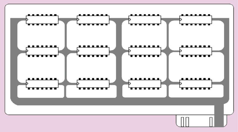
Thus, in a good high-speed design, it is required to provide as many alternate parallel paths to the ground currents as possible. If this concept is extended without limit, it would mean an infinite number of parallel paths that can be approached by using a ground plane. Multi-layer boards, which use an entire plane as ground, can drastically reduce such problems in one fell swoop.
But if one is constrained to use a two-layer board, this effect can be achieved to some extent by using a gridded ground system (Fig. 1). A good rule to follow could be to have a ground track beneath each IC along its length. The vertical spacing would be equal to the length of each IC. The vertical and horizontal traces can be on opposite sides of the board, the tracks being connected at each crossing by printed-through-hole method.
In a typical two-sided board with 15 ICs, it has been found that the ground noise voltage decreases to a tenth when gridded ground system is used. Hence all digital PCBs should have a gridded ground plane.
Reduction of loop area
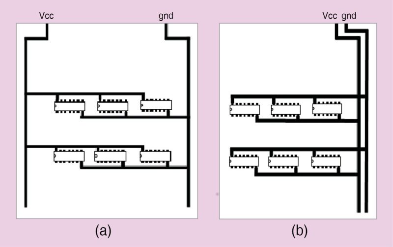
Another method of reducing the inductance is to reduce the area of the loop enclosed by current flow from Vcc to ground. A large open loop (as compared to track dimensions) like that shown in Fig. 2(a) is an efficient radiator of high-frequency currents and the circuit will also be susceptible to externally generated magnetic fields.

For two identical parallel tracks, one for power (Vcc) and the other for ground, which carry currents in the opposite directions, the total inductance (Lt) is given by the expression:
Lt = 2 (L–M)
where L is the inductance of each track and M is the mutual inductance.
Now, if mutual inductance is maximised by keeping the Vcc and ground tracks close together, the effective inductance will be reduced to almost half. Ideally, the Vcc track should follow the ground track on the PCB. This greatly reduces track length, and also the reduced loop area greatly reduces associated emissions and susceptibility issues.
Fig. 2(a) shows a poor PCB layout while Fig. 2(b) shows an improved PCB layout. By reducing loop area we have reduced track length and associated track impedance, and by doing so we have achieved a reduction in emissions and susceptibility
Reservoir/decoupling capacitors
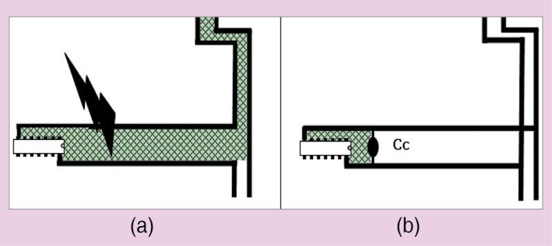
As shown in the Fig. 3(a), even if ground and Vcc tracks are placed close to each other, a high transient switching current is drawn all the way from the power supply rails, causing a large loop of high current (shown by shaded region), which can radiate. If ceramic reservoir capacitor Cc is placed near each IC between power supply and ground tracks, it supplies this short-term switching current and reduces the length of tracks over which this high current flows.
The value of this capacitor (also called decoupling capacitor or decap) should ideally be around 1nF. The capacitor should be of ceramic type as these are capable of releasing their charge at whatever rate required. This and their lower self inductance makes these ideal candidates for decoupling function.
In a board consisting of a large number of ICs (more than 15), the decoupling capacitor of each IC needs to be recharged and the recharging may occur at a considerable low frequency. A bigger bulk decoupling capacitor is often required to supply charging currents to all the decoupling capacitors. The value of this capacitor should be at least ten times the sum of values of all decoupling capacitors. All bulk decaps must have low series inductance; tantalum or metallised poly-carbonate capacitors are best suited for such applications
Common impedance coupling in PCBs
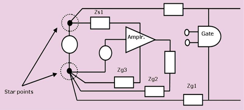
Fig. 4 shows an example of common impedance coupling in a shared power bus wherein an analogue amplifier is shown sharing common power supply and ground tracks with a logic gate. The impedances of supply and ground tracks have been shown as lumped impedances (Zg). At higher frequencies, the impedances of the tracks increase many times, not only because of increased inductance but also because of increased resistance (due to skin effect). This causes an increase in the impedance of the supply tracks.
As we have seen earlier, ground bounce occurs whenever a logic gate switches state. A part of the supply line impedance (Zg3) is common to both the amplifier and the logic gate, so the amplifier will see the ground bounce as noise across power supply and the ground connection. This noise may be transferred to the amplifier circuit either directly through the power supply rails or through the common impedance Zg3, and the noise voltage across Zg3 appears directly across the amplifier input. To reduce the common-impedance coupling we can either reduce the magnitude of the common impedance or remove it entirely.
Eliminating common impedances
The common impedances can be eliminated by using single-point or star connections between power supplies of different circuits. This can be achieved by grouping circuits depending upon their susceptibility (and emissions). Each circuit has multi-point grounding, but the groups use star connections while connecting to common power supply and ground rails. This method is called hybrid connection. The second approach is to use separate power supplies for separate circuit groups, which provides even better isolation between circuits.
This article is an extract from a book by the author. The next part will cover multi-layer PCB designing.
The next part is available at: Electromagnetic Compatibility: Multi-Layer PCB Designing
Chetan Kathalay is working as scientist in Electronics Test and Development Centre, Pune. He is BE in electronics from Nagpur University


Sir can i get this complete book ??? MAil me this book at [email protected]
Hi Asif, you can read this article from our magazine Electronics For You.