


Part 1 of this article in previous issue explained the creation of schematic and PCB layout. This part covers the remaining steps for making PCBs photographically at home, starting with the preparation of the artwork.

Step 3: Prepare the artwork
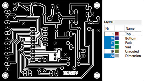
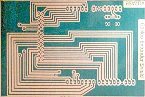
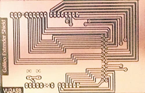
Before you prepare the artwork for transferring the layout to the pre-sensitised PCB laminate, it will be worthwhile understanding how the technique for making PCBs photographically works. For positive-acting type boards, you need a positive artwork film (see Fig. 21), which means that areas where you want to retain copper would be black and opaque to UV light. The UV light passes through the artwork and strikes the material where you want to remove copper, chemically changing the photographic material coated on the PCB such that it becomes soluble in the photoresist developer solvent. This exposes the underlying copper, which is removed by the etching process as described later.
Use A4-size transparencies that were traditionally used for preparing OHP presentation slides. These are readily available at most stationery shops for around ₹ 5 apiece. Ideally, you should use transparencies specially made for laser printers, but these are not so readily available and cost ₹ 50 to ₹ 100 per piece.

Print the artwork through a laser printer. Use the setting for the darkest printout on a black-and-white laser printer. The best results are, however, achieved by using a colour laser printer set to print in colour mode at the highest quality setting. This ensures that multiple layers of colour ink get deposited on the transparency, making the dark areas of the artwork absolutely opaque.
Just to reiterate, the final success largely depends on the quality of artwork you prepare. This means that you need a clear and sharp image for the artwork, which has black areas solid black and opaque to UV light.

Tips, pitfalls and workarounds
Before taking the final printout on a transparency, take a printout on a plain paper and place some components on it to ensure that there is no scaling done either inadvertently or by the software. This is a vital step as many people end up making great looking PCBs only to realise that component pads do not match pins of the actual components.
Many printers produce printouts that are really not dark enough and do not have enough ink deposited on the transparency to make black areas opaque to even ordinary light, leave alone UV light. I usually take four copies of printed transparencies, align them one on top of another and then glue them together on the area around the artwork. This provides excellent results. You must invest time to carefully inspect your artwork.
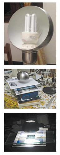
Create two stacks of books and place them about 20cm (8 inches) apart (see Fig. 22).
Place a rectangular piece of transparent glass on top of the two stacks so that it bridges them. Place a small LED or CFL bulb below the glass. Place a transparency on top of the glass and inspect it, preferably with a magnifying glass. Use a permanent marking pen with a small tip to correct any black area that is not dark or opaque enough. When done, stack up the second transparency on top of the first one and carefully align them. Then use fast-setting glue to stick the two aligned transparencies outside of the artwork area. Repeat the process for the other two transparencies. Now you should have a sharp and opaque artwork.
Step 4: Transfer the artwork
Before you transfer the artwork onto the PCB laminate using a UV light source, cut the pre-sensitised PCB board to a size slightly bigger than the boundary of the artwork. Take a 20x25cm2 (8×10 inches2) rectangular piece of Perspex (or plastic or Bakelite) sheet and a transparent piece of glass of the same size around 4mm thick. Using double-sided tape, stick the laminate side of the board onto the Perspex sheet.
Next, you need to place the artwork on top of the PCB side covered with the protective opaque sticker. The correct way to do this is to have the side (surface) of the transparency on which the artwork is printed (ink deposited by the laser printer) to face and touch the PCB. This ensures that the orientation of the artwork is correct and the ink on the artwork touches the pre-sensitised side of the artwork, leaving no space for light to ‘ooze’ or ‘creep’ in between the ink on the transparency and the laminate. Align the artwork to the PCB.
Use a regular (one-sided) piece of tape to stick one edge of the artwork to the Perspex sheet, forming a kind of hinge. So, when the opaque sticker is eventually removed, the artwork is positioned correctly on top of the sensitised surface of the PCB.
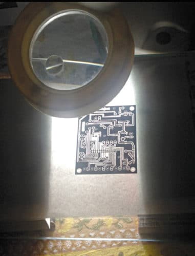
Now you are ready to expose the PCB. The apparatus I used was an 11-watt CFL bulb fitted in an ordinary reading lamp (see Fig. 23). Natural light can expose (and harm) the pre-sensitised board, so perform this step either at night when there is no natural light or in a dark room setting during the day. In fact, just as a sidebar, even sunlight can be used to expose the PCB, but this method is contingent on getting the settings right for the amount of sunlight and the duration of exposure. You can use a small red-coloured bulb in the working area without harming the PCB. Now arrange the apparatus as shown in Fig. 23, ensuring that the CFL is around 5cm above the glass.
It will be nice if there is someone to help you hereafter. Keep a timer next to you; I used the timer utility on my smartphone. Before exposing the PCB, switch on the CFL bulb for around 30 minutes while keeping your sandwich away from it in a dark area. Next, in a dark room setting, slowly remove the protective opaque sticker, ensuring that the PCB does not move from its place.
Ensure that the artwork is aligned with the PCB. Place the glass piece on top of the artwork. Then either use rubber bands or the commonly available paper binder clip to hold the sandwich together. This will ensure that the glass presses the artwork flush against the PCB which has been fastened to the Perspex sheet. Just to reiterate, the final sandwich will have the glass on the top, the artwork transparency below it touching the PCB’s photo-sensitised side with the laminate’s back against the Perspex sheet.
Next, switch off the CFL bulb, arrange the sandwich and the table lamp. Switch on the CFL bulb while setting the timer for 10 minutes. After the time elapses, turn off the light and prepare for the next step.
You must be wondering why to use a CFL bulb instead of a UV light source. There are two reasons: One, CFL bulbs also emit some UV light along with the visible light. Two, these are readily available. The text on the protective foil of these PCBs states that you can expose them either using UV light for a duration of 60 to 90 seconds or use a CFL bulb for six to ten minutes. That suggests that the quantity of UV light emitted by a CFL bulb in a time window of around 10 minutes is equal to that from a UV bulb in around 90 seconds.
Step 5: Developing
During the ten minutes you turn on the CFL bulb, prepare fresh ‘developer’ solution. To do this, take a photographic developing tray. If that’s not available, use a plastic or glass container with a capacity of about 750ml and dimensions of around 15x20cm2 (6×8 inches). Pour 200ml of water in the container. Add half a teaspoon of caustic soda (NaOH) flakes to the water and stir the solution until the flakes fully dissolve in the solution. Ensure that you do not exceed the caustic soda quantity. As caustic soda is a hazardous chemical, use protective gloves and spectacles. You may be able to purchase caustic soda online if you look for flakes of drain cleaner for making soap. Alternatively, try at the local departmental store.

Note that the sequence is critical. Never put caustic soda first and then add water, as it may cause spurting and even violent eruption. If you use caustic soda in powder form, the solution will be too weak to develop the PCB.
After ten minutes of exposing the PCB laminate, shut off the CFL bulb and, in a dark-room setting, carefully remove the glass and the transparency to remove the ‘developed’ PCB. Immerse the PCB in the developer solution in the container with the pre-sensitised side of the PCB facing upwards. Keep stirring the solution; preferably with a 1cm broad hobby paint brush. PCB tracks will soon start becoming visible as green lines.
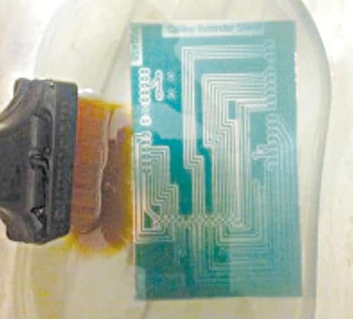
It may take as much as ten minutes to develop the PCB completely; the time may vary depending on the strength or potency of the flakes and the resulting developer solution. Patience is the key here; do not be tempted to add more flakes to accelerate the development as it may ruin the PCB. Continue stirring the developer solution until the PCB looks like the one in Fig. 26. It is fully developed now.
Remove the PCB and rinse it under running water. Wipe the PCB with a tissue paper and let it dry. Carefully inspect the PCB with a magnifying lens. If there is an undesirable bridge formed by the hardened green developer, remove it carefully using a sharp object like a pin. If copper is exposed in an area where it should not be, touch it up using a permanent marker pen with a narrow nib. You are all set for the next step now.
Step 6: Etching
There are several options for etching or removing the exposed copper from the PCB. I had a lot of ferric chloride (FeCl3) solution, so I didn’t look beyond it. FeCl3 is available from chemical shops in the form of crystals and liquid. Please use protective gloves and spectacles for this step. If you have ferric chloride in crystal form, prepare the etching solution by adding 200 grams of FeCl3 crystals in one litre of distilled water. Be cautious while handling it and use either glass or plastic to stir. Ferric chloride should not come in contact with skin. Do not spill or throw it away here and there as it will leave ugly, brown colour stains.
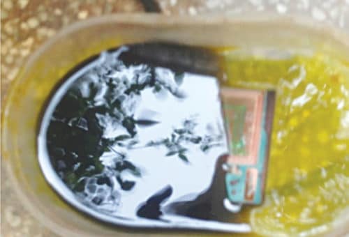
Remove the developer solution from the container, wash it well and pour around 200ml of ferric chloride (etchant) in it. Immerse the developed PCB into the etchant and continuously shake it slowly to ensure that the solution is swished from the PCB surface and fresh solution replaces it. Green-coloured areas on the PCB resist the etching solution and the exposed copper gets dissolved in it. This takes around 10 minutes. Remove the PCB and rinse it under running water. The etched board would look as shown in Fig. 28.
Step 7: Removing the masking material
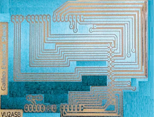
Use a piece of cotton cloth dipped in nail polish remover to remove the blue-coloured toner polymer coating from the PCB.
Some nail polish removers are acetone based, and though these serve our purpose well, they are less commonly available. Many nail polish removers use a mix of ethyl acetate (solvent for nail polish) and isopropyl alcohol. This is a milder chemical but is commonly available and delivers equally good results.
You may also use a paint thinner. This step will result in a PCB as shown in Fig. 29.
Step 8: Drilling holes in the PCB
This is a critical step. The size of the holes and their precise location on the PCB are two most vital aspects you need to address. For most components, 1mm hole diameter is sufficient; some terminal blocks and diodes may need a hole diameter of 1.2mm. This aspect is not difficult to take care of. Maintaining the exact distance between holes required for multi-pin components like ICs and header blocks, though, is very crucial. The slightest misalignment of holes will make it very difficult to even push the component in its destined place.
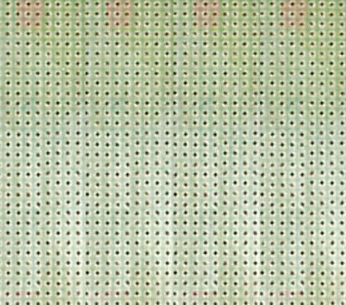
Tips, pitfalls and workarounds. I use a good-quality general-purpose PCB as a former for drilling holes on the newly etched PCB by aligning two farthest placed pins of the component pad centre. This gives excellent results. The boards have 1mm diameter holes, which are spaced 2.54mm apart. Eagle uses a pitch of 0.05 inch or 1.27mm by default in the board layout view. Interestingly, most of the components have pins spaced by multiples of 2.54mm. This makes these boards ideal for use as a former.
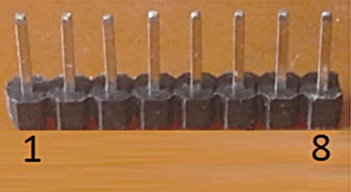
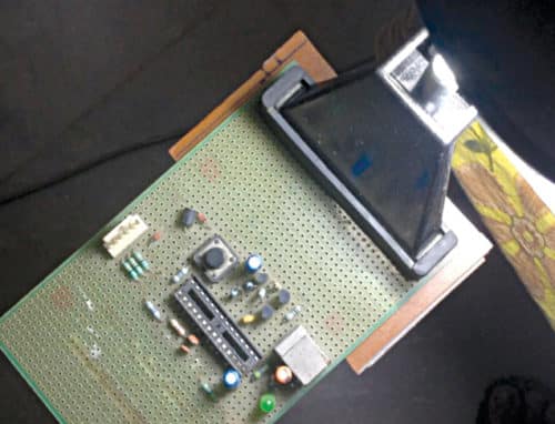
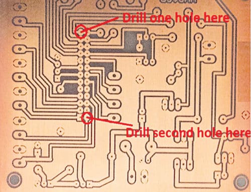
Let’s go through this step by step. Get a general-purpose PCB like the one shown in Fig. 30. Now let’s say you want to drill holes for an 8-pin single-in-line header like the one shown in Fig. 31. Place the copper side of the general-purpose board against the copper side of the PCB and align the two holes you just made with the corresponding holes on the general-purpose PCB (see Fig. 32). It is important to use this PCB orientation because it ensures that the drill bit makes almost perfect holes without damaging the copper pads.
Cut two pieces of a 15mm long and 0.9mm thick wire. If that’s not available, use 0.8mm thick tin wire as hookup wire. Push one piece of the wire through the first hole and the other one through the eighth hole. Now squeeze the two PCBs using a small bench vise; preferably one with rubber lips, as shown in Fig. 33.
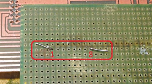
Now using a mini push hand drill, create holes between the first and eighth pins by placing the drill bit in the six holes on the general-purpose board, one at a time. Release the vice, remove the two pieces of the wire and release the two PCBs. Now place the 8-pin header in the holes just drilled. It should fit perfectly.
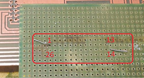
To drill holes for a 26-pin dual-in-line header like the one shown in Fig. 35, identify the diagonally opposite pads as shown in Fig. 36. Now drill 1mm holes at the centre of the two pads as precisely as you can. Hold the two PCBs together with their copper sides facing each other. Cut two pieces of 0.8mm tin wire, used as hookup wire, 15mm long. Now push one piece of the wire through the first hole and the other one through the 14th hole, which is diagonally opposite to the first hole as illustrated in Fig. 34. Now squeeze the two PCBs using a small bench vise; preferably one with rubber lips. Now using a mini push hand-drill drill the balance 24 holes as before.
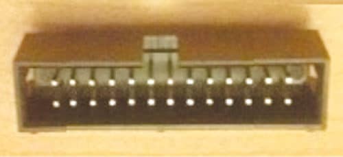
Release the vice, remove the two pieces of the wire and release the two PCBs. Now place the 26-pin header in the holes just drilled. It should fit perfectly.
Drill all the required holes for the PCB. When done, carefully use very fine sand paper to smoothen the copper side of the PCB. Do not rub too much as the copper pads or tracks may get damaged.
Copper starts oxidising fast. So if you wish to store the PCB for a while, place it in a plastic zipper bag after applying transparent lacquer spray on the copper side. Before use, just wipe the lacquer with nail polish remover.

Why all of you making this articles just don ‘t ever finish it ? All of you explain how to make the pcb and how to drill… but most important thing like final art of soldermask , the final look lasting for years…dead subject. How and where to choose materials from so many variants and sellers that sucks …dead subject. But full of articles how to make holes with a drill. Nice.
At every new article about making PCB at home I go to the last page looking for final chapter- How to really do at home the solder mask. Disappointed, always MISSING.