


It is predicted that there will soon be 25 billion permanently-connected sensors to implement the Internet of Things (IoT) in real time. But the challenge is how these devices connected across the globe in different environmental conditions will be powered?
In many cases, power from the grid or large batteries to power up these sensors would not be available. In that case, an ultra-low-power converter to step up the power from ambient energy sources seems to be a perfect solution.
An ultra-low-voltage converter can be defined as a converter that can boost very low input voltage autonomously without any external power supply. The ultra-low-voltage converter can step up input voltage as low as 20mV.

Energy harvesting power sources get more interesting for supplying ultra-low power sensor circuits instead of batteries as shown in Fig. 1, which looks like an attractive and free option.
However, power management required for each sensor, data-processing units and embedded processors is a critical task, as availability of this free energy is uncertain and very low in power. This article describes a power converter circuit that can be used to step up very low power using a self-oscillating circuit.

System block diagram for energy scavenging using an ultra-low-voltage converter is shown in Fig. 2. In this article, each block (of the block diagram) is modelled in LTspice to observe the results in simulation. Detailed description is given below.
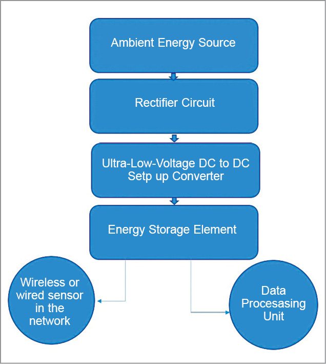
Radio frequency (RF) energy, pressure and temperature are some ambient energy sources. These possess very high internal impedance and, hence, produce output in milli-volts. This output can be boosted to 3V to 6V range, which could be used to drive low-power sensors and embedded processors.
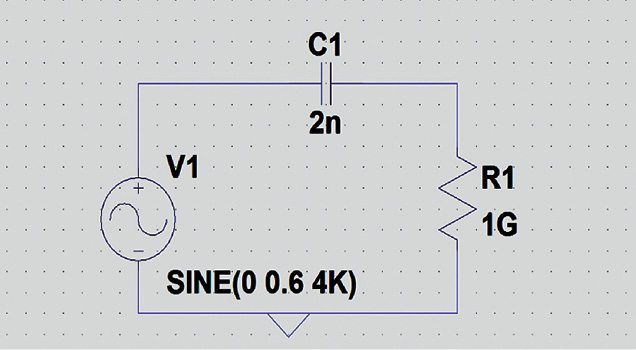
Energy source. RF waves are emitted by TV or radio-broadcasting antennae. These travel very long distances and so can be used for powering remotely-placed wireless sensors. Output of these high-frequency, power-carrying RF waves is found to be as low as 600mV. Ambient energy source model is shown in Fig. 3.
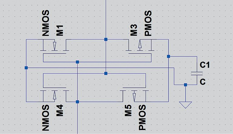
AC-to-DC converter. Output from RF antenna is given to bridge rectifier to convert it into constant DC supply voltage. A diode bridge rectifier can be used for rectification purpose here. But output of an AC-to-DC power converter would be as low as 600mV, which is not sufficient to turn the diodes that have 700mV forward-voltage drop across these. To reduce forward-voltage drop, we can use MOSFET based bridge rectifier circuit, which works perfectly under very-low-voltage input conditions (Fig. 4).
DC-to-DC converter. The converter used here is not a normal step-up converter. It has to step up very low input voltage autonomously. This self-powered converter is based on a self-oscillating circuit like Armstrong oscillator. Advantage of this circuit is ultra-low-input voltage and high-voltage stepping-up capability.
An oscillating circuit is mainly used as a kick-start of a main converter because of the need to skip external-regulated voltage. Most self-oscillating circuits work at mill-watt power levels. Armstrong oscillator based converter topology is shown in Fig. 5. For such a system, energy source, which is an antenna, has a large internal impedance (up to several kilo-ohms).
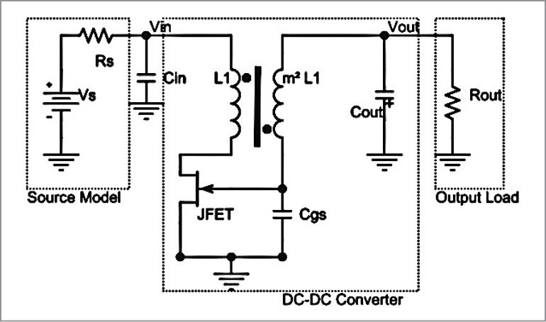
Working of the self-oscillating Armstrong converter topology is described below:
Oscillator. It is formed by junction field effect transistor (JFET) and amplifies gate input signal. Oscillator feedback loop is formed with two inductors, which are coupled, and gate-source capacitor Cgs.
Rectifier. To rectify JFET’s gate-oscillating voltage, gate-source PN junction of JFET is used. When JFET’s gate voltage becomes greater than diode-threshold voltage, the diode is turned on and circuit supplies output to load. When the power converter is connected to an energy source, current rises in the primary winding. Secondary winding provides a positive gate voltage on n-channel JFET.
Here, it is assumed that JFET is already on. So Cgs connected to gate terminal of JFET is charged to a positive (Vgs) value. Gate source PN junction of JFET is forward-biased because of enough gate supply voltage given by the capacitor; output capacitor (Cout) is charged with a negative voltage.
Output voltage is therefore negative. When primary current reaches saturation, primary winding voltage gets cancelled and output capacitor delivers a negative voltage to JFET gate to make it pinch off.
Current in the primary winding decreases and negative voltage is applied to JFET gate, which finally switches off the JFET. This peak voltage that switched off JFET falls back to zero, that is, secondary winding current reaches zero value and gate terminal gets rid off the negative voltage earlier applied across it.
Again, JFET gets turned on and the procedure repeats, thus oscillation process gets started.
Main advantage of this circuit is in ultra-low-voltage applications. This circuit has a forward mode of operation. Energy is transferred to output during on phase, which avoids the collapse of the switch-gate voltage oscillations during off-phase (a case of fly-back operation mode).
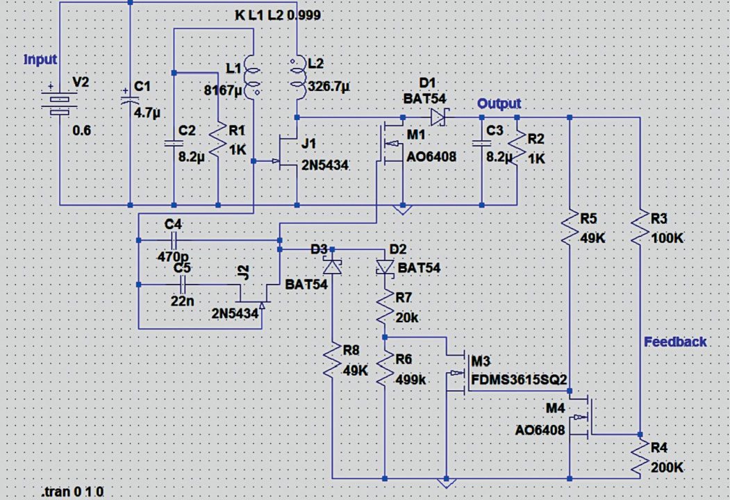
The self-oscillating ultra-low-voltage converter circuit simulated in LTspice is shown in Fig. 6. For simulation:
1. Download LTspice version 4 for Windows or MAC OS
2. After installing the setup file, click on ultra_stepup_converter.asc file given at the end of the article. It will automatically open in the software and you will find the schematic capture window (Fig. 6).
3. Run the schematic by clicking the icon on the left-hand corner and you will get the results.
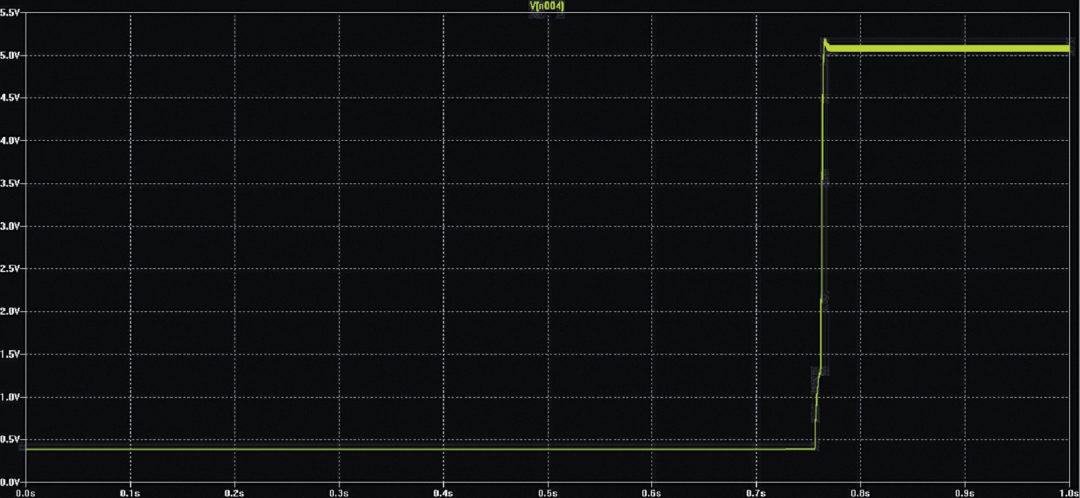
A self-oscillataing converter is capable of boosting 0.6V to approximately 5V. Output power is around 22mW and input power around 23.4mW. Simulation output of the system is shown in Fig. 7. Overall converter efficiency is about 92 per cent in simulation environment.
Energy storage. Energy storage will supply power to the sensor, microcontroller or data transreciever module. Advantages of the super capacitor make it ideal for energy storage. However, it takes a lot of time to charge and discharge.
Some semiconductor manufacturers have already introduced ultra-low-power ICs, which are capable of boosting as low as 10µW of input power. At such low input power, efficiency, noise immunity and stabilty of a power converter become questionable. But advancements in technology would definitely help future implementation of the IoT easy and reliable.
Rohan Kadam is passionate about electronics and new technologies. He likes reading articles on application of power electronics and embedded systems, writing technical and non-technical articles

Please I am looking for Mtech Electronics 100 Pages Project.
thanks
Sorry, we cannot help you personally but we’d recommend you to join our forum (https://www.electronicsforu.com/forums) and post your question there. Our community members could help you out. Registering is just one-click and free through ‘FB Connect’. You could also post your question on our timeline.
may i know how do you calculate the values needed for this converter?