


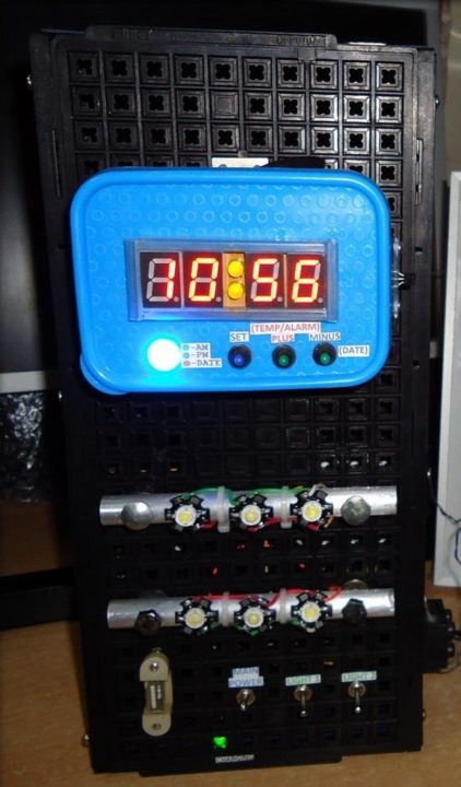
Building clocks are one of the interesting and easiest projects that can be seen among hobbyists and makers. Presented here is a multifunction rechargeable clock unit that not only functions as a clock but also as a rechargeable light lantern and a mobile charger. The clock has all the basic functions like date-time display, alarm and room temperature display. The clock is powered through a lead acid battery which can be recharged through solar power or mains power supply so that the clock never ever runs out of power.
The clock is also provided with a female USB socket which can be used to charge most of our mobile phones and gadgets. It has a dedicated battery charging and load cut-off circuitry that takes care of the battery through exact charging topology and prevents it from being overcharged or getting undercharged.
Block Diagram
The functional unit of the clock is divided into two units namely power unit and the main clock unit. The block diagram of the power unit is shown in figure 1.

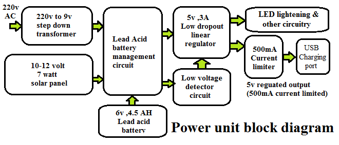
The main aim of the power unit is to provide continuous power to the clock and further circuits. In this process, a lead acid battery is being charged which powers the circuits ahead.
The lead acid battery can be charged via two sources namely solar power and mains power.

Battery management circuit
The battery management circuit is so designed that it accepts power from two sources at the same time but gives priority to the main power such that if solar power is low or unavailable, user can plug it into the mains wall supply to charge it. A solar photovoltaic panel is used to directly convert solar light and heat energy into electricity.
To harness the mains power into meaningful power, a step down transformer is used which converts high voltage AC into low voltage AC. This AC voltage is rectified and converted into DC, and then further smoothened by using capacitors as low pass filters. After this, the power becomes acceptable to be fed to the battery management circuit.
The lead acid battery is directly connected to the battery management circuit which takes cares of charging the battery and maintaining its charging voltage and current to acceptable limits that ensures longer battery life, capacity and optimum usage.
Comparator circuit
Next we have used a comparator circuit which checks the battery voltage against its internal reference voltage and shuts-off the load thus preventing battery from further discharging. Then a linear low drop out regulator is used to derive regulated 5v rail from the battery rail. This 5v rail is non-current limited and powers most of the circuitry ahead like lightening LEDs, etc.
A current limited load switch is used to derive a 5v rail which is current limited to 500mA for USB charging applications. We have current limited this rail to 500mA for USB charging applications to prevent USB application from immediately discharging the clock battery.
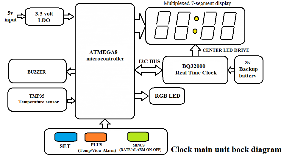
The block diagram of the main clock unit which comprises of the microcontroller section is shown in figure 2.
Microcontroller section
Here the brain of the circuit is the microcontroller which keeps track of all the sensors and switches connected to it, makes decisions and calculations, and finally updates the display section. The non-current limited 5v rail from the power section is converted into 3.3v rail in this section via a 3.3v LDO regulator which powers the microcontroller and other peripherals. To sense the room temperature, a temperature sensor is provided whose output is an analog signal proportional to the temperature. This signal is fed to one of the analog to digital converter channel of the microcontroller.
The user inputs are sensed by three momentary push to on switches which are used to set/check various parameters of the clock like alarm, date, etc. The time keeping is done by a separate real time clock (RTC) chip which is interfaced to the microcontroller via I2C bus. The RTC is also powered by a backup battery which keeps the time running even if the main power fails.
The display section comprises of the four 7-segment displays which are multiplexed to efficiently use the limited pins available on the microcontroller. The two center LEDs between the two pairs of seven segment displays are driven by the RTC clock. A RGB LED is also provided to display indications of AM/PM and date display. At last, a buzzer is provided to acknowledge user button presses and to depict alarm states.
Power Unit Circuit
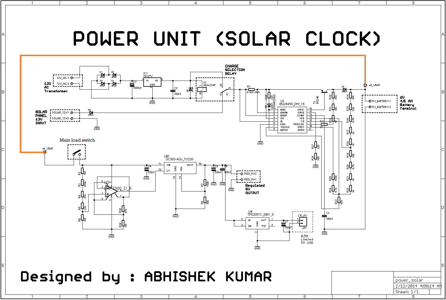
The circuit diagram for the power unit is shown in figure 3.
The mains 220v AC is first converted into 12v AC using a step down transformer. This 12V AC is converted into approximate 17V DC using diodes D1-D4 which are used in bridge configuration. This DC is further smoothened using a 1000uF electrolytic capacitor which acts as a first order low pass filter. Ceramic capacitor C2 is used for further stability of the LM7812 regulator.
A LM7812 linear regulator is used to derive regulated 12v DC which is fed to the relay coil and also to the normally open contacts of the relay K1. A 10-12 volt, 7 watt solar panel is used to obtain electricity from sun’s energy. The electric power from thesolar panel is fed to the normally closed contacts of the relay with a bypass diode D6 in series
Circuit operation
As this diode D6 will create a drop in voltage after the solar panel’s output, so it is recommended to choose a diode which has the least forward dropout voltage such as schottkey diode 1N5822.The diode D5 which is connected in parallel to the relay prevents the back emf of the diode to harm the rest of the circuitry.
Now as the solar panel’s output is fed to the normally closed contacts of the relay so when mains power is not available, the relay will be turned off and thus solar panel’s power will directly feed the charging circuitry. When mains power is available, it will turn the relay ON and thus the mains derived 12v DC will pass through the relay cutting off the solar panel’s power. This way during low solar power hours or night times, the user can charge the clock using mains power.
Now the common terminal of the relay goes to the charging circuitry which comprises of the bq24450 IC from Texas instruments. The bq24450 contains all the necessary circuitry to optimally control the charging of valve-regulated lead-acid batteries. The IC controls the charging current as well as the charging voltage to safely and efficiently charge the battery, thus maximizing battery capacity and life.
Circuit specifics
For our application, the IC is configured as a simple constant-voltage float charge controller for 6v, 4.5 AH battery. The bq24450 IC is so flexible that it can be programmed in various configurations to suit different charging currents and voltages for batteries of different capacities. Only an external pass transistor and minimum number of external passive components are required along with the IC to implement a charger for sealed lead-acid batteries. Here in our configuration, a PNP transistor T1 (BD240) is used to drive the battery charging power. Before going into the programming of battery charger, let us define the required parameters for our battery.
- Final discharge voltage (Vth) = 1.75V per cell = 5.25V
- Float voltage (Vfloat) = 2.30V per cell= 6.9V
- Voltage in boost mode (Vboost) = 2.45V per cell = 7.35V
- Charge rate can be 0.05C to 0.3C
- We will use charge rate (IMAX-CHG) = 0.13C = 600 mA (approx)
- VBAT (MIN) =4V
- Trickle charge rate = 10 mA
Programming parameters
Now we will go through the various programming parameters required for implementing a dual level charger for our battery chemistry. The first step is to decide on the value of the current in the voltage divider resistor string in FLOAT mode. This should be substantially higher than the input bias current in the CE and VFB pins and the leakage current in the STAT1 pin, but low enough such that the voltage on the PGOOD pin does not introduce errors. A value of 50μA is suitable.
Let us say,
RA = R14+R15+R16+R17+R18
RB = R19+R20+R21+R22
RC = R23
RD = R24+R25
RP = R27+R28
In FLOAT mode, STAT1 is OFF, so there is no current in RD. The voltage on the VFB pin (VREF) is 2.3V
RC = 2.3V ÷ 50μA = 46kΩ The closest 1% value is 47kΩ.
VFLOAT = VREF × (RA + RB + RC) ÷ RC
RA + RB = 2 × RC = 92.8kΩ.
VBOOST = VREF × (RA + RB + RC//RD) ÷ RC//RD
RD = 474.3kΩ.
VTH = VREF × (RA + RB + RC//RD) ÷ (RB + RC//RD)
RB = 16.9kΩ,We choose closest 16.7k
RA = 92.8kΩ – RB = 75.9kΩ, choose closest 75.7k
IPRE = (VIN – VPRE – VDEXT – VBAT) ÷ RT. Thus, RT = 634Ω,we choose closest 639Ω
The charging current for the battery is programmed by selecting the right value of the shunt resistor R1.Thus
IMAX-CHG = VILIM ÷ R1
R1 = 250mV ÷ 600mA = 0.417Ω. The closest 1% value is 0.422Ω.
RP = (VIN(MIN) – 2.0V) ÷ IMAX-CHG × hFE(MIN) = 7 ÷ 0.6 x 27 = 320Ω.
Circuit connections
LED1 in the bq24450 circuitry displays the state of charging. The schottkey diode D7 again serves the role of preventing the back current leakage from the battery and after that the circuit feeds the lead acid battery. After this stage, the battery rail goes to the low voltage detection circuitry and the UCC383 LDO in series with a SPST load switch. The battery low voltage detection circuit is built around the comparator LMP7300 which has an internal reference of 2.048 volts. The low voltage of the battery at which the it should be disconnected from the load is deemed to be around 1.75 v per cell which estimates to 5.25volts for three cell battery.
The comparator output is open collector and the circuit is so designed that its output goes low when the battery voltage drops below 5.25 volts. The output of this comparator goes to the enable pin of the LDO in next stage. Thus whenever the battery voltage goes below 5.25 volts, the output of comparator goes low which in turn switches the LDO off and thus shutting down all the load OFF from the battery and preventing it from getting further discharged.
The potential divider network comprising of the resistors R2 to R6 establishes a voltage of 2.048 volts at the non-inverting terminal of the comparator when battery rail reaches to 5.25 volts which is compared with the inverting terminal of the comparator which is directly connected to the reference output of the LMP7300. Further a combined negative and positive hysteresis of about 300mV in total is programmed to the LMP7300 through R29 and R30 so that the comparator output does not fluctuate when the battery voltage reaches the exact crossing point of the reference potential of the comparator.
The LDO UCC383 is capable of driving loads upto 3A with a maximum dropout of 0.45 volts which is excellent for our application. The Vin pin accepts the battery rail which nominally varies in the range of 6 to 7.5 volts while charging and 5.25 to 6 volts while normal usage.
Through R7 and R8, the output voltage of the LDO is set to 5 volts. C4, C5 and C6 are used for stability purpose of the LDO. The 5 volt rail thus obtained will be used to power most of the circuit. TPS2051C which is a 500mA current limited load switch from Texas Instruments is used to drive a 500mA current limited 5volt rail which will be used to power/charge USBapplication. We have used a current limited load switch so as to prevent the USB application from fastly draining the clock battery however this feature is optional. C7 is again used here for stability purpose of the current limiter.
Power LED & USB charging connections
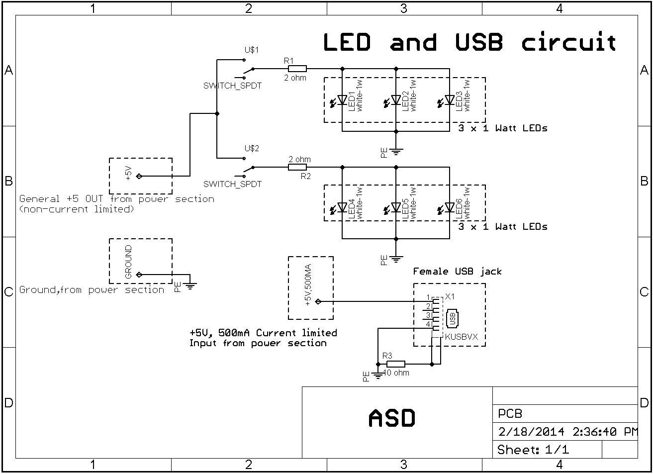
The circuit connection for the power LEDs and USB charging socket is shown in figure 4.
Here two pairs of 3 x 1watt power LEDs are used for lightening application. A current limiting resistor of 2 ohms is used to limit current in each pair of LED channels in series with a SPST switch. These two LED channels receives power directly from the non current limited 5 volt rail (from the power unit section). A female USB-A type jack is used here for USB charging applications which receives power from the 500mA, 5v current limited channel (from power unit section).
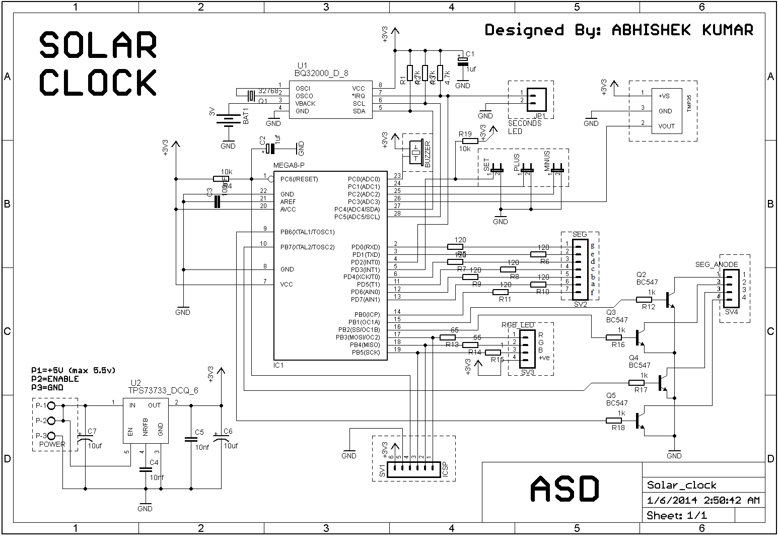
The circuit diagram for the microcontroller based main clock circuit is shown in figure 5.
Multifunction rechargeable clock circuit
The circuit is responsible for implementing a clock which, apart from general time display also features alarm function and indication of date, month, year and temperature. The circuit is built around the famous ATMEGA8 microcontroller from ATMEL. ATMEGA8 is responsible for performing display updation, sensing user inputs/sensors and performing required decision making.
Microcontroller
The ATMEGA8 provides the features like 8 Kbytes of In-System Programmable Flash with Read-While-Write capabilities, 512 bytes of EEPROM, 1 Kbyte of SRAM, 23 general purpose I/O lines, 32 general purpose working registers, three flexible Timer/Counters with compare modes, internal and external interrupts, a serial programmable USART, a byte oriented Two wire Serial Interface, a 6-channel ADC with 10-bit accuracy, a programmable Watchdog Timer with Internal Oscillator, an SPI serial port, and five software selectable power saving modes.
A separate in circuit serial programming port SV1 is available for programming the microcontroller. The time keeping is done by the RTC chip bq32000 from Texas Instruments. The bq32000 features an automatic backup supply using a 3v battery.
The bq32000 has a programmable calibration adjustment from –63 ppm to +126 ppm, so that it can also be used with low quality crystals. The bq32000 includes automatic leap-year compensation. The RTC chip is connected to the microcontroller via the I2C bus and in this project uses a 3v CR2032 lithium cell for the backup supply. For the functioning of the internal oscillator, a 32.768 KHz crystal is used at OSC0 & OSC1 pins. The IRQ pin on the RTC chip is connected with ATMEGA8 on PIND.2 and is also responsible for driving the two middle LEDs which are located between the two seven segment display pairs. The anodes of two yellow colored LEDs (in parallel) are connected to this IRQ pin while the cathode to ground on the JP1 socket.
Temperature sensor
Three momentary push to ON switches namely SET, PLUS and MINUS are connected to the pins PD.3, PC.1 and PC.2 respectively. An analog temperature sensor TMP35 from Analog Devices is used for room temperature sensing. The TMP35 analog signal output is proportional to the temperature by the relation 10mV/degree Celsius which is interfaced to the analog to digital converter on the microcontroller. The sensor is connected on the ADC channel 3 (ADC3) on ATMEGA8. A beeping buzzer is connected to the PC0 pin which will be used for acknowledging the user inputs and for alarm indication.
Display
For display, four multiplexed common cathode displays are connected to PORTD and PORTB on pins 2, 3, 6, 11, 12, 13 and 14 and their individual cathode pins are connected to the SV4 jack which are driven by four NPN transistors. A RGB LED is connected to PB3(red), PB4(green) and PB5(blue) pins on the controller. The RGB LED is employed here to indicate AM/PM and date on the display unit. The active low reset pin on the ATMEGA8 is pulled up by a 10k resistor and also tied to a 1uf electrolytic capacitor for stability purpose to prevent the controller from regenerative resetting during supply transients. The AREF pin which is the reference in/out pin for ADC is tied to a 100nF ceramic capacitor for stability purpose, while the AVCC(20) and AGND(22) pins are the power supply pins for the ADC circuitry on the microcontroller.
Pins VCC (7) and GND (8) are the power pins for rest of the circuitry on the microcontroller. It is important to note that we are using the internal 1MHz RC oscillator on the ATMEGA8 for its functioning hence we do not need to connect any crystal to the microcontroller, and it is important to set correct fuse bits on the ATMEGA8 to configure it for 1MHz internal RC oscillator. For powering the clock circuit, a 3.3v LDO TPS73733 is used which gets its input from non-current limited 5v rail from the power section. The TPS73733 is a 3.3v, 1A regulator with a maximum input voltage of 5.5volts. The EN pin is used for enabling the LDO, however here we have tied it directly to the Vin pin for continuous operation.C5, C6 and C7 are used here for stability purpose of the LDO. An external capacitor C4 to the NR/FB pin on the LDO bypasses noise generated by the internal bandgap, reducing LDO output noise to very low levels.
Display connections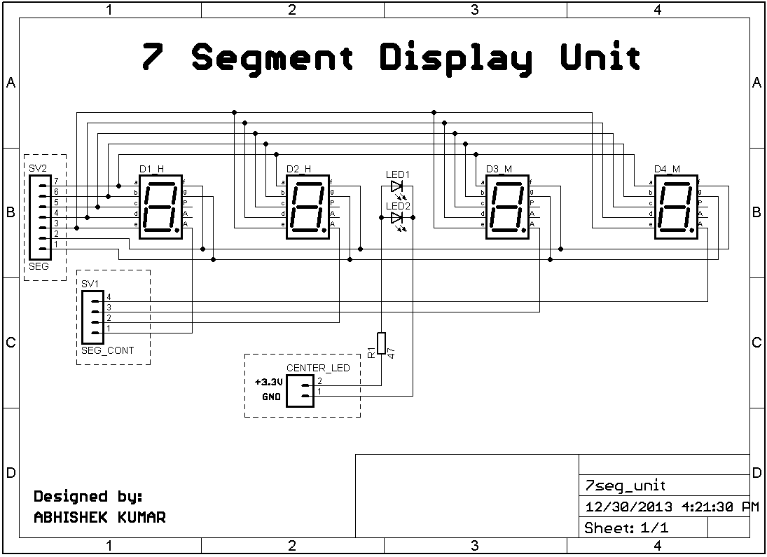
Figure 6. Multiplexed seven segment display unitThe circuit diagram for the multiplexed seven segment display unit is shown in figure 6.
This circuit contains four seven segment displays arranged in pairs of two, two in left side for displaying variables like hours, date, etc and two in right side for displaying variables like minutes, month, etc. Connections on SV1 and SV2 go to the display driving ports on the main clock section. Two middle LEDs with a 47ohm current limiting resistor in series are provided for indicating whether time or other data is displayed on the seven segment displays.
Microcontroller code
The code for the ATMEGA8 microcontroller is written in BASIC language using the BASCOM-AVR compiler from MCS electronics. Initiating the code, we allocate default values to the eeprom from location 1 to 4.
The eeprom is basically used to hold the user settable alarm values. Starting from first location holds the alarm hours, then alarm minutes, then alarm PM and at last the alarm flag which indicates whether alarm is ON or not.
Then we declare some subroutines to clear seven segment displays, reading RTC chip, display value setting, etc. After this, we configure the ADC to run in single mode with auto prescaler and using internal 2.56v reference. We configure the directions of input-output ports and initialize them. The I2c pins are configured and initialized.
Then we initialize timer0 for multiplexing the seven segment display, timer1 for handling alarm duration and timer2 for blinking the segments while the clock is in “Settings” mode.
After this we declare and initialize certain variables for ADC calculations, time seeking, etc. Doing all that, now we initialize the I2c pins, read the eeprom contents for alarm values and initiate an infinite loop where the RTC chip is read and displays are updated continuously.
Also in the same infinite loop, the user inputs are acknowledged and associated event are initiated like setting alarm ON/OFF, displaying date-time, etc. Also, the current time is compared against the alarm variables and alarm is initiated when the time is matched.
It is important to note here that while burning the hex file “solarclock.hex” to the microcontroller, the eeprom file “solarclock.eep” must also be programmed to the microcontroller.
Using the clock
The clock can be charged from solar power as well as mains power. A 10-12v, 7 watt rated solar panel should be installed on top of the roof in such a direction so that it can receive enough power throughout the day. The connections from the solar panel should be carefully routed to the clock charging terminals keeping in mind the correct polarity. Although solar power is more than enough to provide continuous power to the clock forever, and the clock can last for more than 60 hours on single charge. But during peak times when solar power is not available like in cloudy days or night, user can charge the clock using mains power.
The solar panel is automatically cut-off while charging through mains power. This way the clock will never ever run out of power. The mains load switch can be used to cut-off all the load from the battery. The two 3 x 1watt LED modules can be individually switched ON according to the needs. And using the USB jack, user can charge all possible USB applications thus the project also functions as a solar powered USB charger. The charging status is indicated by LED1 in the power unit, where glowing LED means the battery is being charged. The power unit circuit has the feature to automatically shut-off the load when the battery voltage reaches the state of discharge.
The clock will automatically switch ON after switching ON the mains load switch. The user interface of the clock is designed in such a way that only three buttons are used to set the various parameters like current time, hours, date-time, etc and to display the current date-time, set alarm, room temperature, etc. It is to note here that the “PLUS” button can be used to increment the values in “Settings” mode. Also pressing it once during normal time display mode, first displays the room temperature and then the set alarm values. After that, it reverts back to normal time display with an acknowledgement beep.
Similarly the “MINUS” button can be used to decrement the values in “Settings” mode. Also pressing it once during normal time display mode, first displays the current date on left and current month on right, and then the current year. After that, it reverts back to normal time display with an acknowledgement beep. To switch ON/OFF the alarm, simply press the “MINUS” button for more than 1 second, and if the display indicates “AL-0” means alarm is turned OFF while “AL-1” means alarm is turned ON.
To set the various parameters of the clock, pressing “SET” button once will bring it into settings menu. In the settings menu, “PLUS” and “MINUS” keys are used to increment and decrement the current value respectively and the corresponding pair of seven segment displays will start blinking. Pressing the “SET” button again will bring the clock into next parameter setting mode and so on until the normal time is displayed. On pressing the “SET” button once, the following seven setting are noticed which can be changed by the user:
1. SET CURRENT HOURS
( AM/PM can be set by overflowing/underflowing the hours)
2. SET CURRENT MINUTES
(After setting the current hours and minutes; “SET” is displayed on the display)
3. SET MONTH
4. SET DATE
5. SET YEAR
(After setting month, date and year; “SET” is displayed on the display)
6. SET alarm hours
( AM/PM can be set by overflowing/underflowing the hours)
7. SET alarm minutes
(After setting alarm hours and minutes; “SET” is displayed on the display)
To switch off the running alarm anytime, any of the three buttons can be pressed once. Green color on the RGB LED indicates AM, blue indicates PM and red indicates that date is displayed.

how to use the sorce code it was not opening???..
Dear Aswanth Sai, could you please check it again. From our side the source code is opening.
Hello,
Thank you
Would you sell this kit?
Kit isn’t available for this project. But you may visit kitsNspares.com where you can get wide range of DIY projects with all required components and PCB.
I need this project
Explain about this
Kindly elaborate your query.