
Microcontrollers such as Arduino and ESP32 are excellent for building embedded projects, but they reveal only one part of digital system design. Inside every modern processor, FPGA, AI accelerator, and System on Chip, thousands of hardware blocks must exchange data quickly and efficiently. Managing this communication has become one of the biggest challenges in chip design.
How modern chips move data internally
Instead of relying on a single shared bus that quickly becomes congested, modern chips use Network on Chip (NoC) architectures that route data much like a computer network. These tiny hardware routers allow multiple processing blocks to communicate simultaneously, improving performance, scalability, and power efficiency.
Building a simple NoC router is one of the best ways to understand how modern processors, AI chips, and multicore systems move data internally. In this project, the router is designed in Verilog, introducing the core concepts of hardware description, packet routing, arbitration, buffering, and parallel data transfer that form the foundation of FPGA and ASIC development.
What is a Network on Chip router and why is it needed?
Inside a chip, there are many small blocks (like processors, memory units, etc.) that need to send data to each other. If all of them try to use a single shared connection (bus), it quickly becomes crowded and slow, like multiple devices trying to send data over a single USB cable one after another. As the number of blocks increases, this quickly becomes a bottleneck.
To overcome this limitation, modern chips use something called a Network-on-Chip (NoC) architecture, where data is sent through small packages, similar to how messages travel through routers on the internet.

A NoC router acts like a traffic manager that receives small pieces of data (called flits), checks where they need to go, stores them temporarily if needed, and sends them in the right direction. If multiple data packets want to go to the same place, it decides who goes first and who waits.
This project includes a basic NoC router in Verilog to understand how modern chips manage internal communication. It shows how data moves inside a chip and how conflicts are handled, making it easier to understand how larger systems are built.
Learning outcomes
This project will give hands-on experience in designing digital systems using Verilog, understanding how data is stored, routed, and managed inside hardware. It introduces key concepts like buffering, routing, and arbitration while also building practical skills in simulation, waveform analysis, and hardware debugging. Most importantly, it gives a clear insight into how scalable communication works inside modern chips.
Bill of Materials
This project requires only free and open-source software tools, making it easy to build.
Icarus Verilog (iverilog)
An open-source Verilog simulator used to compile and simulate the router design.
Download:
- macOS: brew install icarus-verilog (terminal command)
- Windows: Download from SourceForge. (Icarus Verilog download | SourceForge.net)
Visual studio code (VS code)
A lightweight code editor used to write and manage Verilog files. (Download Visual Studio Code)
Project Overview
The router receives data from multiple directions and decides where each packet should go, controlling the traffic, resolving conflicts, and forwarding it to the correct output.
The data arrives at five input ports (North, South, East, West, Local) and is stored in queues. The router reads the destination, generates requests, arbitrates if multiple packets want the same output port, and finally routes the selected packets through a crossbar, allowing parallel data transfer in each clock cycle.
Data(Flit) format (32-bit)
Data moves through the router in fixed-size packets called flits.
| Bits | Function |
| 31-28 | Destination field |
| 27-0 | Payload data |
Destination encoding
| Output port | Code |
| North | 1000 |
| South | 0100 |
| East | 0010 |
| West | 0001 |
The router examines these bits to decide where each flit should go.
Router Architecture
The Network-on-Chip (NoC) router operates in six well-defined stages, each responsible for a specific function in transferring data from input ports to output ports. This staged design simplifies understanding, debugging, and future scalability.
The router consists of the following functional blocks.
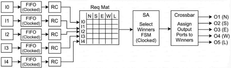
(All codes are available in the GitHub repo)
Stage 1: Input ports
The router consists of five input ports (I0–I4). Each input port receives incoming data packets (flits) from neighbouring routers or local processing elements.
At this stage:
● Flits arrive asynchronously from the external environment
● No routing or arbitration is performed yet
● The flits are simply presented to the router for buffering
Stage 2: FIFO buffers (Clocked)
Each input port is connected to a FIFO (First-In-First-Out) buffer, which is a clocked storage element.
Functions of this stage:
● Temporarily stores incoming flits
● Handles congestion when outputs are busy
● Decouples input arrival from output availability
Flits are written into the FIFO on the rising edge of the clock and remain there until they are granted access to an output port.
Implementation:
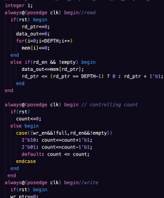
The FIFO uses three separate always@(posedge clk) blocks for write, read, and count, making each operation easy to follow independently. The count register tracks occupancy directly, so full and empty are simple comparisons rather than pointer arithmetic.
Write and read pointers wrap around using a conditional instead of modulo, since hardware synthesis of % is expensive. On reset, all memory slots are cleared in a loop, and both pointers return to zero.
Stage 3: Route Computation (RC)
The Route Computation stage examines the flit at the head of each FIFO. In this stage:
- The destination field of the flit is extracted
- The target output direction (N, S, E, W, or L) is determined
- A routing request is generated for the desired output port
This logic is combinational and continuously evaluates valid FIFO entries.
Implementation:
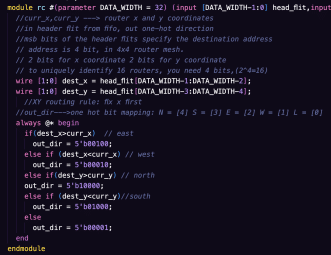
RC uses an always @* block, meaning it is purely combinational — no clock is involved. It reads the top 4 bits of the head flit: bits [31:30] as dest_x and bits [29:28] as dest_y. It then applies the XY routing rule: the X dimension is resolved first (East/West), and only once X matches does it resolve Y (North/South).
If both match, the flit is at its destination and goes Local. This chain of if-else-if priority guarantees exactly one direction bit is asserted in the 5-bit one-hot output out_dir.
Stage 4: Request Matrix formation
The routing requests from all RC blocks are collected into a Request Matrix. Structure of the matrix:
● Rows represent input ports (I0–I4)
● Columns represent output ports (N, S, E, W, L)
Each entry in the matrix indicates whether a specific input is requesting a specific output. This stage makes all routing conflicts explicitly visible.
Implementation:
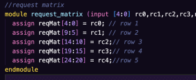
The Request Matrix is entirely wiring — no logic gates are synthesised. Each RC unit outputs a 5-bit one-hot direction. The module simply concatenates all five into a flat 25-bit wire: reqMat[i*5 +: 5] = rc_i.
So reqMat[4:0] holds I0’s request, reqMat[9:5] holds I1’s, and so on. The Switch Allocator then reads this wire column by column — one column per output port — to find which inputs are competing.
Stage 5: Switch Allocation
The Switch Allocator (SA) resolves conflicts. Responsibilities of this stage:
● Inspect requests for each output port
● Select exactly one winning input per output
● Apply a fixed-priority or round-robin policy
● Generate one-hot encoded grant signals
Inputs that do not win arbitration remain safely stored in their FIFOs.
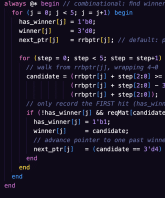
The SA uses round-robin arbitration: one pointer per output port (rrbptr[j]) remembers which input won last time. Each cycle, a combinational always @* block scans up to 5 inputs starting from that pointer, finds the first one with a pending request, and marks it as the winner.
The pointer then advances past the winner so the next competing input gets priority next cycle, preventing any single input from monopolising an output port. The results are registered at the posedge: grant [winner*5 + j] goes high and rrbptr[j] updates. Losers keep their flits in their FIFOs and retry the next cycle.
Stage 6: Crossbar switching and Output assignment
The final stage is the Crossbar switch, which performs the actual data movement.
In this stage:
● Grant signals configure the crossbar
● Winning inputs are connected to their assigned output ports ● Flits are forwarded to outputs O1–O5 (N, S, E, W, L)
● Successfully transmitted flits are removed from the FIFOs. This stage completes one full routing operation per clock cycle.
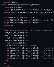
The crossbar is a combinational multiplexer. It loops over all 5 inputs and checks each input’s row in the grant matrix. If grant[k*5 + j] is set, input k wins output port j, and that input’s FIFO head flit is driven onto the corresponding output (out_N, out_E, etc.).
The SA guarantees at most one bit is set per output column, so there is never a drive conflict. All five outputs can be driven simultaneously in the same clock cycle as long as they carry different flits.
Outputs
The file router.v integrates all the 5 modules to make one router. Open router.v and run this code in the terminal:
iverilog -g2012 -o sim router.v
vvp sim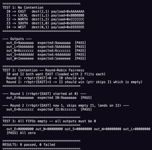
Summary of the 6 Stages
1. Input Ports receive flits
2. FIFO buffers store flits safely
3. Route computation decodes destinations
4. Request matrix collects routing requests
5. Switch allocator selects winners
6. Crossbar forwards flits to outputs
Future, scalability and potential
Although this project starts with a single Network on Chip router, it lays the groundwork for complex mesh and torus topologies used in modern multicore processors, AI accelerators, and System on Chips.
Future enhancements can include Quality-of-Service (QoS) features, such as priority-based routing or virtual channels, to handle varied traffic types.
References
[1] NIT Rourkela, E-Thesis on Network-on-Chip Router Design, 2021. Available: http://ethesis.nitrkl.ac.in/5708/1/e-79.pdf
[2] International Journal of Computer Science and Mobile Computing, NoC Router Architecture, June 2017. Available:
[3] IRJET, Network-on-Chip Router Implementation, Vol. 3, Issue 15. Available: https://www.irjet.net/archives/V3/i5/IRJET-V3I5494.pdf