


Many devices, such as water pumps, exhaust fans, and geysers, need to run for only a limited period. Forgetting to switch them off can result in unnecessary power consumption and wear. This timer system can automatically switch off a garage light after a car is parked or turn off an exhaust fan, water pump, or outdoor light after a preset time, reducing power consumption and wear.
Some applications also require a device to remain off for a few minutes after the power supply is restored. For example, a refrigerator or air-conditioner compressor should preferably not restart immediately. This allows the refrigerant pressure to stabilise and helps protect the compressor from excessive stress caused by rapid switching.
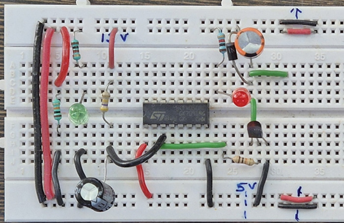
Two simple timer circuits are described here. The first is an on-delay timer that switches on the connected appliance after a preset delay. Fig. 1 shows the author’s on-delay timer prototype assembled on a breadboard.
The second is an off-delay timer, which keeps the appliance on for a preset period and then switches it off. Fig. 2 shows the author’s prototype of the off-delay timer assembled on a breadboard.
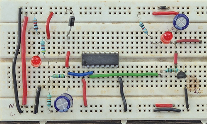
Both circuits use a minimum number of components and are easy to assemble. The delay can be varied continuously from approximately three to fifteen minutes by adjusting potmeter VR1.
Circuit and working
Two types of timers are described here: an on-delay timer and an off-delay timer.
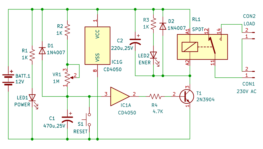
The on-delay timer is built around CD4050 (IC1), a non-inverting hex buffer. The IC contains six buffers, but only IC1A is used in this system.
When the system is powered on, capacitor C1 is initially discharged. C1 starts charging through resistor R2 and potentiometer VR1. The voltage across C1 gradually increases. When it reaches the input threshold of the CD4050, its output goes high. This drives transistor T1, which energises relay RL1. The appliance connected through CON2 is then switched on.
The delay before the relay energises depends primarily on the time required to charge C1 through R2 and VR1. Increasing either the resistance or capacitance increases the delay, while reducing either value decreases it.
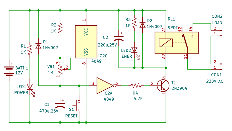
The pinout of the 4049, a hex inverter, is compatible with that of the CD4050 for this application. Therefore, the CD4050 in Fig. 3 can be replaced with a 4049 (IC2) to configure the system as an off-delay timer, as shown in Fig. 4. The IC contains six inverters, but only IC2A is used.
| Parts List (Fig. 3 on-delay timer) |
| Semiconductors: IC1 (IC1A-IC1G) – CD4050 hex buffer T1 – 2N3904 NPN transistor D1, D2 – 1N4007 rectifier diodes LED1, LED2 – 5mm red and green LEDs Resistors (all 1/4-watt, ±5% carbon): R1, R4 – 4.7kΩ R2, R3 – 1kΩ VR1 – 1MΩ potmeter Capacitors: C1 – 470µF, 25V electrolytic C2 – 220µF, 16V electrolytic Miscellaneous: RL1 – 12V SPDT relay CON1, CON2 – 2-pin connectors BATT.1 – 12V battery/12V SMPS supply LOAD – Anything like refrigerator or an AC S1 – Push-to-on switch |
| Parts List (Fig. 4 off-delay timer) |
| Semiconductors: IC2 (IC2A-IC2G) – 4049 hex inverter T1 – 2N3904 NPN transistor D1, D2 – 1N4007 rectifier diodes LED1, LED2 – 5mm red and green LEDs Resistors (all 1/4-watt, ±5% carbon): R1, R4 – 4.7kΩ R2, R3 – 1kΩ VR1 – 1MΩ potmeter Capacitors: C1 – 470µF, 25V electrolytic C2 – 220µF, 16V electrolytic Miscellaneous: RL1 – 12V SPDT relay CON1, CON2 – 2-pin connectors BATT.1 – 12V battery/12V SMPS supply LOAD – Anything like geyser or water pump |
Fig. 4 shows the off-delay timer. It is built around a hex inverter 4049 (IC2). In the off-delay timer configuration, the output of the 4049 is initially high and the relay remains energised. When the voltage across C1 rises above the input threshold of the 4049, its output changes to the low state, switching off transistor T1 and consequently de-energising the relay.
The exact threshold depends on the IC and supply voltage. The delay can be varied by changing the value of C1 or the resistance of R2 and VR1. The charging voltage can also be limited to a fraction of the supply voltage using a voltage divider.
Several additional components are included to ensure reliable operation and provide visual indication. LED1 serves as the power-on indicator, while LED2 indicates that the relay is energised. Capacitor C2 helps prevent relay chatter during switching. Switch S1 is used to provide a discharge path for C1 for quick reuse of the timer.
EFY note. The circuit operates from 5V to 12V. For a 5V supply, use a suitable 5V relay instead of the 12V relay. The 4049 input threshold and CD4050 switching threshold vary with supply voltage, temperature, IC manufacturer, and device characteristics.
Construction and testing
The actual-size, single-sided PCB layout for the on-delay timer is shown in Fig. 5, and the component layout in Fig. 6. After assembling the circuit, mount it in a suitable enclosure. Fix CON1 and CON2 on the rear panel, and switches and LEDs on the front panel. Mount potentiometer VR1 on the front panel for convenient delay adjustment. Fig. 7 is an alternative modified off-delay timer, so its PCB layout is not provided.

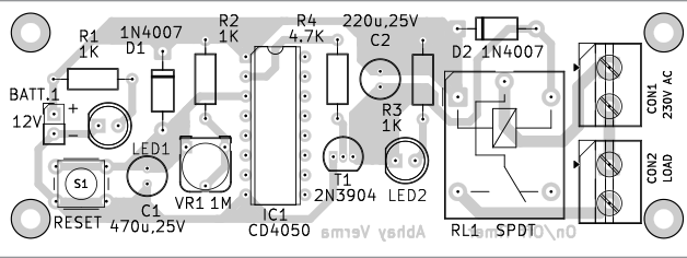
Alternatively, the circuit can be assembled on a Veroboard or general-purpose PCB. A 12V DC SMPS module is recommended for powering the circuit, although a 12V transformer with a rectifier and filter can also be used.
In the on-delay circuit, LED1 glows immediately after power-on, while LED2 glows after the preset delay when the relay energises. In the off-delay circuit, both LEDs initially glow; after the preset delay, the relay de-energises and LED2 goes off. After successful testing, connect the appliance through the relay contacts and a suitable AC outlet.
Caution. The relay contacts may carry mains voltage. Provide proper insulation, enclosure, earthing, fuse protection, and adequate PCB spacing. Never touch the circuit while it is connected to the mains.
Alternative modified off-delay timer
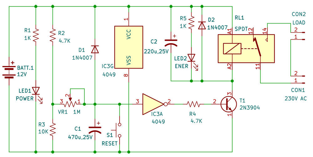
Fig. 7 shows the alternative off-delay timer, which is a modification of the off-delay timer shown in Fig. 4. This is also a 12V off-delay timer using the CMOS CD4049 inverter. When the 12V supply is switched on, C1 starts charging through R2 and VR1. The voltage at the input of IC3A gradually rises. Until this voltage reaches the switching threshold of the 4049, the inverter output remains high, keeping T1 conductive. The timing can be adjusted with VR1, while S1 provides a reset/discharge path for C1. IC3 (IC3A-IC3G) has six inverters, but only IC3A is used.
| Parts List (Fig. 7 Alternative off-delay timer) |
| Semiconductors: IC3 (IC3A -IC3G) – 4049 hex inverter T1 – 2N3904 NPN transistor D1, D2 – 1N4007 rectifier diodes LED1, LED2 – 5mm red and green LEDs Resistors (all 1/4-watt, ±5% carbon): R1, R5 – 1kΩ R2, R4 – 4.7kΩ R3 – 10kΩ VR1 – 1MΩ potmeter Capacitors: C1 – 470µF, 25V electrolytic C2 – 220µF, 16V electrolytic Miscellaneous: RL1 – 12V SPDT relay CON1, CON2 – 2-pin connectors BATT.1 – 12V battery/12V SMPS supply LOAD – Anything like geyser or water pump |
When the input threshold of IC3A is reached, its output goes low and transistor T1 cuts off. Consequently, relay RL1 de-energises, and its contact changes over to disconnect the load. Glowing LED2 indicates that the relay is energised, while D2 protects T1 from the relay coil’s back-EMF when the relay is switched off.
Capacitor C2 prevents relay chatter while diode D1 resets the circuit when power is switched off by discharging the capacitor C1 through R2 and R3. LED1 indicates that the 12V supply is present. The timing is mainly determined by R2, VR1, and C1. Therefore, adjusting VR1 changes the delay. The relay’s SPDT contacts (CON1/CON2) provide electrical isolation between the low-voltage timer circuit and the 230V AC load.
Pradeep Vasudeva is a member of the Indian Forest Service, currently posted as Director State Forest Research Institute, Jabalpur. Electronics has been his passion since adolescence, and his areas of interest include amateur radio, RF circuits, and audio projects.