

 A lot of remote sensing thermometers have a problem with measuring more than one temperature at a time. To overcome this problem, a different technique is adopted here, which allows you to sense eight (at the most) transducers at a time.
The technique
Block diagram of the wireless addressable digital thermometer is shown in Fig. 1. At the transmitting end, an 8-bit analogue-to-digital converter (ADC) continuously scans and converts signals from eight different temperature sensors. The sensors are selected sequentially by a 3-bit binary addressing system. At any moment, output of the ADC is an 8-bit binary number representing the analogue signal developed at the output of a particular temperature sensor, being addressed at that moment.
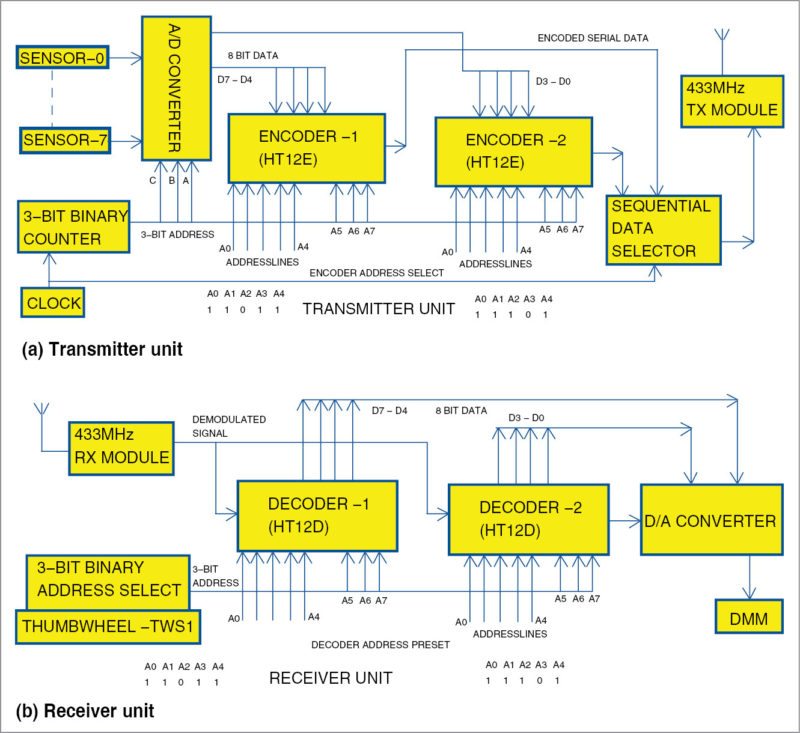
By using special parallel-to-serial encoders, this 8-bit data, along with the binary address of the sensor, is sent serially to the remote receiving end. Communication between the two ends are met with the help of a pair of 433MHz UHF transmitter and receiver modules operating in ASK/OOK mode.

At the receiving end, the transmitted signal is received by a 433MHz ASK/OOK RF receiver module. The received 8-bit serial signal is then converted back to its original parallel form, by using special data decoders as explained later. An equivalent analogue signal is then developed from this data by an 8-bit digital-to-analogue converter (DAC). A digital multimeter connected at the output of the DAC is used to show the temperature on mV scale.
Sensors identification
Scanning of sensors is governed by a 3-bit binary counter, which places, in a cyclic fashion, sequentially-changing binary numbers from 000 to 111 on the three designated scanning input lines, A, B and C, of the ADC. Each number bears the binary address of a particular sensor, and whenever addressed, the sensor sends data to the ADC for conversion to its digital equivalent.

Here comes a problem. Due to continuous scanning of sensors by the ADC, received data may come from any one of the possible eight sensors. Hence, for proper identification of a source sensor, specific 8-bit binary number (address) is tagged with the 8-bit signal output of each sensor, prior to transmission. Special data encoders are used for this purpose.
The encoder used in this system can send only four bits of the 8-bit sensed data at a time. Hence, the sensed 8-bit signal from the ADC is first broken into two nibbles of four bits each. The nibbles are then sent, one after the other, repeatedly to the receiving end, after attaching the said 8-bit address to each of these by the said encoders.
Among the total eight bits of the address word, three are scanning bits, as explained above, and fixed for a particular sensor. The remaining five bits are manipulated to designate two different addresses to two different data nibbles. These five bits, once set, must remain set forever. So, during scanning of sensors, although the logic levels of A-B-C scanning input lines of the ADC go on changing sequentially from 000 to 111 in cyclic order, the said five other bits of the address word remain fixed to their preset value. As a result, different sensor output is allotted with different 8-bit addresses to both nibbles. This is true for all eight sensors.
At the receiving end, after detection, sequentially-received two pulse trains for two nibbles are fed to two special decoders. Like encoders, decoders, too, have pre-settable eight address lines. If at any time, the preset address of a decoder matches with the instantaneous address of an encoder, the decoder decodes the received signal and extracts the 4-bit data sent for it, and consequently places the same on its four output lines.
The 8-bit output data (4-bit plus 4-bit) from the two decoders are fed to an 8-bit DAC. The DAC in return generates an equivalent analogue current. This current, when allowed to flow through a resistor, developes an analogue voltage (negative with respect to ground) across it. This analogue output of the DAC is measured with the help of a digital multimeter.
Circuit and working
Circuit of the wireless addressable digital thermometer is divided into three parts: transmitter, receiver and power supplies.
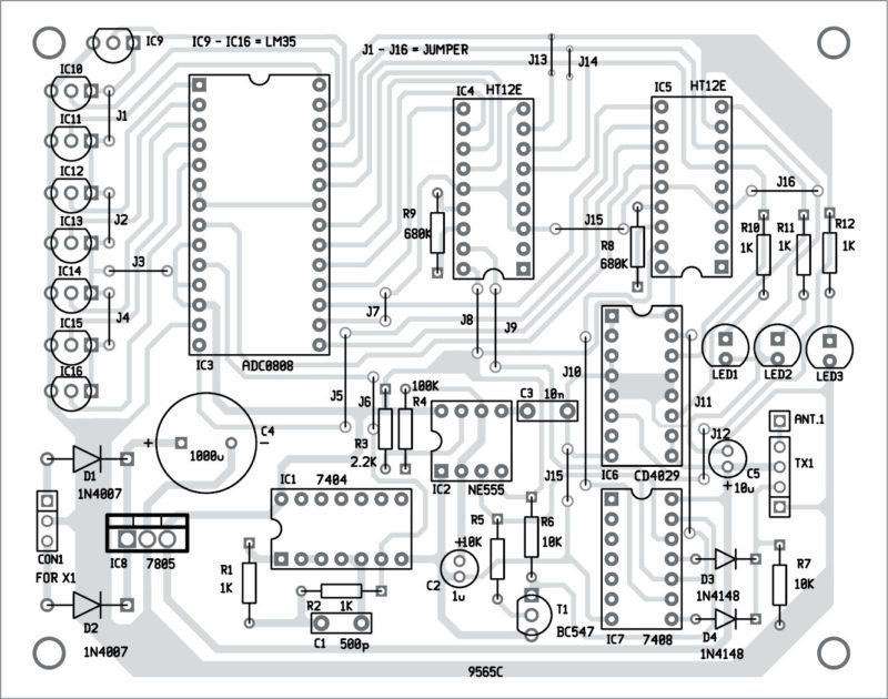
Transmitter. Fig. 2 shows the circuit diagram of the transmitter unit for the wireless addressable digital thermometer. Eight LM35 IC temperature sensors (IC9-IC16) are connected to IN0-IN7 inputs (pins 26 to 28 and 5 to 1) of ADC 0808 (IC3). Although the ADC is capable of accepting a total number of eight sensors through its eight input lines, less number of sensors could be used as well as, whenever desired. IC 7404 (IC1) configured as a CMOS oscillator with the help of resistors R1 and R2, and capacitor C1 feeds the ADC with necessary clock pulses required for conversion processes.
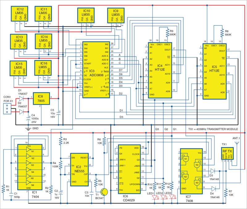
Output voltage of LM35 series IC temperature sensors follows linearly (@10mV/°C) the centigrade temperature of its surroundings, taking 0mV at 0°C temperature. The ADC continuously scans its eight input lines. The scanning process is governed by a 3-bit binary up counter built around CD4029 (IC6).
The counter places a continuously-changing 3-bit binary number on A-B-C input lines of the ADC (pins 25, 24 and 23). Scanning rate is dependent upon the clock constructed around timer NE555 (IC2), and is 8Hz, approximately. Hence, each of the eight sensors is allowed to send data to the ADC for approximately one-eighth of a second, irrespective of whether all sensors are connected or not.
Here, IC3 is configured in continuous operational mode. So, whenever a particular sensor is addressed, output lines of the ADC reflect the present analogue output status of the sensor. Output of the ADC goes to data input lines of special encoders HT12E (IC4 and IC5); higher nibble to IC4 and lower nibble to IC5, respectively.
As TE input (pin 14) of encoders is permanently grounded (logic 0), the encoders are configured to produce encoded data continuously. Data is available at pin 17 of IC4 and IC5. These two encoded digital outputs are alternately steered to TX1 (TX-433MHz), a UHF RF transmitter module, to modulate UHF carrier wave generated by the module. Selection of encoder output is done in the following manner:
Whenever IC2 output pulse goes high, pin 10 of AND gate N3 of IC7 (a quad 2-input TTL AND gate) also goes high, allowing output of IC5 to be steered to TX1 through diode D4. At the same time, due to the presence of transistor inverter T1, pin 13 of gate N4 of IC7 goes low, inhibiting output of IC4 to reach TX1 through gate N4. As soon as the clock pulse returns to logic 0, output of IC4 gets its passage to TX1 through gate N4 of IC7.
So, in essence, analogue data of a sensor is converted and the resultant 8-bit digital data is sent to the remote end using ASK/OOK modulation, in a complete clock cycle of IC2.
Modulated signal is radiated into space through a wire (approximately 35cm long), acting as an antenna, connected at the antenna point of the module.
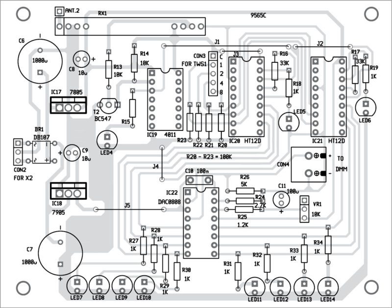
Receiver. Fig. 3 shows the receiving unit of the wireless addressable digital thermometer. RX1, a 433MHz RF receiver module, is used to receive and demodulate ASK-modulated RF signal transmitted by TX1 of the transmitter unit. Demodulated output is a train of rectangular pulses comprising a 4-bit data nibble and destined for a particular decoder as explained earlier.
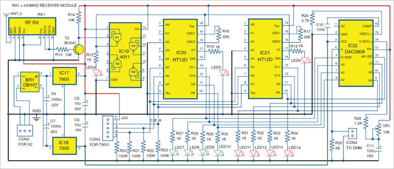
Transistor BC547 (T2) is used as a pulse amplifier to amplify the signal output from RX1 and, hence, raises the pulse height to CMOS compatible logic -1 (>3.5V at 5V). This compatible output is then fed to CMOS NAND gate 4011 (IC19). NAND gate N1 helps to get pulses of perfect rectangular-wave shape. Output of gate N1 of IC19 is fed to decoders HT12D (IC20 and IC21). Address lines of the decoders are preset to receive data from encoders IC4 and IC5, respectively.
LEDs (LED5 and LED6) connected at their VT outputs (pin 17) flicker to indicate reception of valid data. Decoding speed (as measured at pin 15) is 200kHz (approximately). Decoded data is then fed to IC22, a DAC (0808). Analogue current output of the DAC (pin 4) is loaded with resistor R26. Voltage developed across it is fed to a digital multimeter, which shows the temperature on mV scale.
A thumbwheel switch (TWS1) is used to change the preset address of the decoders (IC20 and IC21). The switch changes the last three LSB of the address. For example, to get data from the sensor (IC13) connected at IN4 input of the ADC, the number to be set on TWS1 is 4.
Power supplies. The thermometer needs power supplies both for its transmitter and receiver units. Whereas the transmitter unit needs only a +5V regulated power supply built around X1, D1, D2 and IC8 (Fig. 2), the receiver unit needs a dual +5V and -5V supplies built around X2, BR1, IC17 and IC18 (Fig. 3). Both circuits work from 230V AC, 50Hz connected to the primaries of transformers X1 and X2, respectively.
Power supply circuits are self-explanatory. Three-terminal positive voltage regulator IC 7805 is used both in the transmitter and the receiver units to get regulated +5V supplies. On the other hand, a three-terminal negative-voltage regulator IC 7905 is used to get -5V supply required for DAC0808 of the receiver unit.
Construction and testing
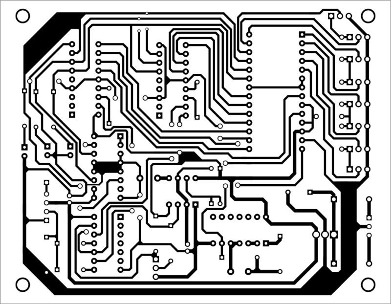
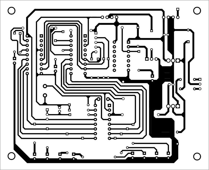
An actual-size, single-side PCB pattern for the transmitter unit of the wireless addressable digital thermometer is shown in Fig. 4 and its component layout in Fig. 5. Similarly, an actual-size, single-side PCB pattern for the receiver unit is shown in Fig. 6 and its component layout in Fig. 7.
Download PCB and component layout PDFs: click here
For connection of TWS1, use a four-wire cable to connect it to the PCB. Fix TWS1 on the front panel of the receiver unit.
Mounting of the sensor IC requires some special attention. If temperature of a solid surface is to be monitored, the sensor may be fixed to the surface by using metal clamps, or glued directly to the surface with high-temperature epoxy adhesive.
For liquid temperature measurement, the sensor cannot be immersed directly in the liquid, as the liquid may be a conductive type, and in that case, the sensor’s leads would be electrically shorted. To solve this problem, the sensor may be mounted inside a sealed-end metal/glass tube. Connecting wires must go to the leads through high-temperature insulating sleeving. The tube may then be dipped into the liquid, or screwed through some threaded hole in the container of the liquid. Although steel gives very high ruggedness to construction, in general, a glass tube would be an ideal choice when temperature of a chemically reactive bath is to be measured.
During construction, special care must be given regarding the choice of some resistors and capacitors. Resistors R1, R2, R24, 25 and 26 must be of highly-stable and low-temperature co-efficient type, to make the units stable against time and ambient temperature variations. Metal-film type may be used for this purpose. VR1 is a 10-kilo-ohm, 40-turn trim potmeter. This should be of highly stable type.
Ground return leads of the sensors must be grounded close to ADC ground lead, otherwise erroneous results may be observed.
Calibration and adjustment
For proper operation of this wireless thermometer, reference current (to pin 4 of DAC0808 – IC22) of the receiver unit should be pre-adjusted. To do this, follow the steps below:
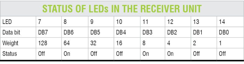
Connect a known voltage source (not exceeding +5V) to any input of the ADC, say, at IN6 (pin 4) of the ADC. Switch on the transmitter unit. Connect a DMM across R26 of the receiver unit. Set the range switch to DC 200mV range, positive lead to ground and negative lead to top of R26. Switch on the receiver unit. LEDs at decoder outputs should start glowing to indicate the received voltage data. If source voltage is 1.5V, status of LEDs should be as listed in Table I.
So, received voltage = (D× 5)/256 = (76×5)/256 = 1.50
where D is the weight of the binary numbers represented by LED7 through LED14.
Now, adjust trim potmeter VR1 to get 150.00mV on the dial of the multimeter. Connect another voltage source at the input and see that the multimeter shows it correctly. If required, re-adjust the trim potmeter. After proper calibration, enclose the circuit in two separate boxes with suitable connections of input and LED indicators.
How to use
1. Attach LM35 sensors (IC9 through IC16) of the transmitter unit to different subjects of interest, noting inputs (IN0-IN7) of the ADC to which these are connected individually.
2. Attach a digital multimeter to the output of the receiver unit with positive lead to ground and negative lead to R26. Set the multimeter’s dial to 200mV range.
3. Switch on both transmitter and receiver units.
4. Rotate the rotary thumbwheel switch to get the temperature of a particular subject. For example, if you like to get temperature of the subject attached to the sensor connected to IN6 input of the ADC, the thumbwheel switch ought to be rotated to position 6.
5. A temperature of 27.5°C would be displayed as 27.5mV (when value of R26 is around 500-ohm). If R26 is 5k, displayed value would be 0.275V when DMM range switch is set to 2V.
Applications
Although the system can be used best to measure temperatures in hazardous or inaccessible areas (like a radioactive zone), the same can also be used by a hospital doctor to monitor, from a fixed location, the body temperatures of multiple patients lying in different rooms without visiting each patient in person.
A hotel control room can monitor temperatures of all the rooms at the same time by using multiple units. The unit can also be used (with certain modifications) as a wireless digital voltmeter.
Arup Kumar Sen is a retired technical officer – II, S.A.I.F., Bose Institute, Kolkata