AI has transformed software development. Is Hardware productivity next? An Indian startup is building an AI helper that works inside PCB tools to place and route boards automatically.
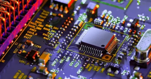
PCB design still takes weeks of manual effort. Placement, routing, power planes, iteration cycles, and rework can stretch development timelines from months to half a year. AutoCuro Technologies, founded in 2024 in Delhi by Manav Marwah and Gaurav Arora, is building an AI assistant to reduce this effort.
The product is not yet available in the market. Speaking about the expected launch timeline, Manav said, “We are working to complete the updates, finish testing, and release the product soon in 2026.”

Autocuro is not another EDA tool. It is an AI layer that sits on top of existing design environments like KiCad, Altium Designer, and Cadence Allegro. It acts as a local AI assistant installed on a designer’s system.
Once a schematic and board outline are ready, the tool:
- Understands schematic context automatically
- Identifies power nets, buses, high-speed signals
- Performs intelligent component placement
- Generates routing and power planes
- Runs DRC checks and cleanup
Unlike traditional auto-placement tools that treat every net equally, AutoCuro analyzes circuit intent. It understands why a crystal must sit close to a microcontroller, how power domains should be separated, and how differential signals should be handled. The result is clear. You get a structured, context-aware placement that mirrors how a human engineer thinks.
Most AI PCB tools operate in the cloud. AutoCuro runs locally. This matters for enterprise teams that cannot upload proprietary designs. The assistant installs as an executable file and works directly with existing EDA tools, protecting company IP. It does not replace engineers. It accelerates them.
PCB placement and routing are moving toward an AI-first approach in the coming years. As AI takes over the repetitive groundwork, engineers will focus more on validation, optimization, and design decisions that require experience and judgment. The company is building this shift step by step, starting with placement and routing today and gradually expanding toward handling more complex PCB designs in the future.