


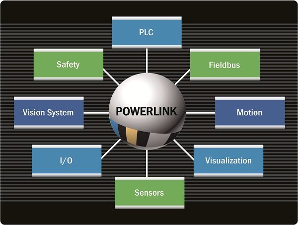
Many Indian OEMs and device manufacturers are looking at incorporating Ethernet POWERLINK technology in their devices to achieve higher performance, throughput and accuracy at the same time a lowest total cost of ownership. There are many reasons for the selection of Ethernet POWERLINK as a communication technology for their systems working as controllers, motion controllers, sensors or field devices. The few benefits which can be sited – Open source, availability of complete master and slave source codes free of cost, no copyrights and no licenses, no hardware modifications needed on master and slave side, using standard Ethernet, compliance with IEEE 802.3 and IEC standards, no limitation of the hardware and software used in the system, deterministic real time communication characteristics, low cycle times down to 100µs, availability of redundancy and many more.

POWERLINK, the only open source deterministic solution

“The reign of proprietary systems for industrial electronics is over. Openness and real independence from these manufacturers makes it easy for device manufacturers to integrate POWERLINK cheaply and easily. They enjoy this freedom of implementation with the choice of hardware and software at their disposal” says Ninad Deshpande, Specialist – Open Technologies. “In less than a decade Ethernet POWERLINK has created a strong foothold in the Indian market with more than 150,000 nodes installation at various plants. These nodes encompass controllers, remote I/Os, drives, sensors and actuators. Device manufacturers in India too have realized the benefits of the technology and expressed their trust in the open source stack. Absolutely no licenses and no copyrights!” Ethernet POWERLINK, which is a real time open source solution, is used as a communication backbone in systems. POWERLINK is the world-wide leader for real time Ethernet solutions. As of 2015 it has an installation base of over 1.1 million systems and 3200 OEMs trusting in POWERLINK.
Ethernet POWERLINK Standardization Group (EPSG) is a consortium of these 3200 members and users worldwide. Thus the technology is not owned by any single organization. The Ethernet POWERLINK Standardization Group was established as an independent association in Winterthur, Switzerland, in 2003. Since its inception, this association of commercial companies, research institutes and end users has focused on the effective exploitation of Ethernet’s benefits for high-performance real-time network systems. The EPSG acts on behalf of its members and advocates their common interests to standardization bodies and associations. In addition, it certifies approved devices. Their active involvement in the EPSG and influence on standardization also gives users and manufacturers an effective means to ensure they are making safe investments.
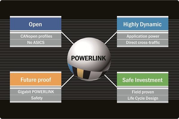 POWERLINK is the only real-time deterministic solution based on standard Ethernet and is truly open source solution in the market. Here, determinism is defined as the ability of a network to send a piece of information to a specific destination and receive a response in a time frame that is predictable and repeatable. With the rapid evolution of Ethernet from Mbits/s to Gbits/s and further with POWERLINK, the user safeguards and future proofs his investment as POWERLINK is ready for these evolutions. Thus, any standard PC, any industrial PC or embedded chip having an Ethernet port can be used to run POWERLINK without any hardware modifications and it is a complete software solution. It is possible to run POWERLINK on any hardware but below we are providing the 5 easy steps to runopenPOWERLINK stack on an Altera FPGA.
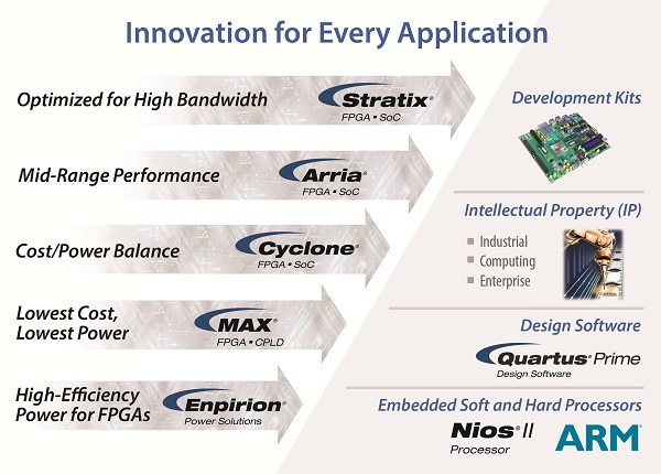
FPGAs are enabling innovations across industries. A wide range of critical application demand usage of FPGAs and are in use in fields of wireless communication, optical transport networks, computer and storage, military and aerospace, automotive and industrial automation. OEMs from all verticals can benefit from the completely hardware independent implementation of POWERLINK and Altera provides a perfect FPGA platform for its effective implementation. “We at Altera provide a flexible platform to support multiple protocols on a single platform. In an attempt to ease customer efforts for implementing POWERLINK we provide the complete solution from silicon to software stacks that are fully tested and ready to use” quotes Prasad Reddy, FAE Manager, South Asia Pacific, Altera India. Altera offers a slew of FPGAs, SoCs with embedded processor systems, CPLDs, ASICs and complementary technologies such as power solution that meet the different price, power and performance needs for the customers. Altera SoCs integrate an ARM-based processor system with all the required peripherals for the processor and FPGA fabric with all interconnects. This enables the customers to build their entire system on the SoC with increased system performance, reduced power consumption, reduced board size and overall reduced system cost.

Getting started with Altera FPGAs
Step 1: Understanding the technology and specification
For those who are interested in getting started with implementation the first step is to understand the technology and how it functions. POWERLINK being an open source technology has the specification and the technology documents available online: click here. provides varied documents for downloading. They vary form specifications, implementation guidelines, whitepapers and much more. These documents will provide the device manufacturer complete knowledge of the technology and communication methodology.
Step 2: Accessing the source code
The Ethernet POWERLINK Standardization Group (EPSG) is responsible for managing the source code.The device manufacturers can download the source code along with the demo examples from the website which also has extensive documentation about the technology. As of April 2016 openPOWERLINK stack version 2.3.1 is the latest version available. The stack is updated with newer features and newer design platform on a periodic basis with a well-documented revision history. Extensive documentation for the implementation is available: click here
Step 3: Working with Altera FPGA platforms
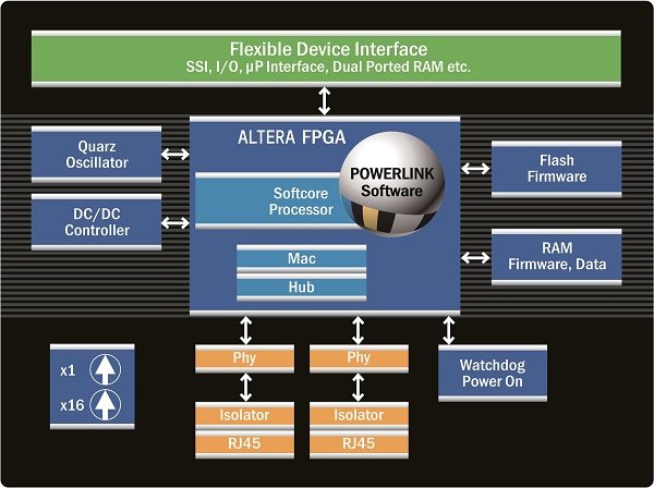
The source code of openPOWERLINK is readily available for Cyclone 4 and the Cyclone 5 SoC chips from Altera. The stacks and application example are tested and available online with the XDD file associated with the development board. In case the device manufacturer selects Cyclone 4 series then he can proceed with the Cyclone 4 development board and can implement the master stack or the slave stack on the chip depending on his requirements. The procedure for setting up the master stack are provided at the location whereas the procedure for setting the slave stack are provided at the location. If the device manufacturer finalizes on the Altera Cycle 5 SoC then he can use the Altera Cyclone 5 development board and the procedure for setting up the master stack are provided at the location.
The source code is built with Altera Quartus 2 v14.0.200 for the Cyclone 5 SoC and with Quartus 2 v13.0 SP1 for the Cyclone 4. A step by step procedure is available at the above mentioned linksfor building and downloading the stack for the above mentioned platforms.
The source code, applications and design for the above two platforms are maintained online and all newer features are incorporated during the version upgrade. In any case if the device manufacturer wants to use any other chips such as the MAX10, Stratix or any chip from the Altera portfolio then he needs to download the openPOWERLINK stack available online and port the stack to the required chip. During porting he needs to update the pin assignment, modify the Ethernet driver and update the addressing depending on the selected chip. The pin assignment and addressing could also change if the manufacturer uses any other version of the Quartus 2 software for the readily available platforms. Thus the user either needs to use the defined Quartus 2 version as defined in the documentation or needs to make necessary modifications while using the newer version of the Quartus 2 software. If the users uses the Quartus 2 v15.0 for building the Cyclone 4 or Cyclone 5 SoC then the building could throw up errors. Thus the user needs to use Quartus 2 v14.0.200 for Cyclone 5 SoC and V13.0 SP1 for Cyclone 4 as the pin assignments addressing for the FPGAs is as per this versions. Any change in versions could lead to errors which the user needs to resolve for completing the building process.
Step 4: Support for the technology
When any device manufacturer starts’ working with any new technology it is bound to happen that he would have questions and could require support. To help the device manufacturers we have an active forum which is responsible for answering to the questions raised. The support questions are answered by technical experts for different organization and they can be raised at the following location on the website. There are different sub heading under which the user can post his comments – getting started, porting, technology, and open discussion. Raising question and posting to any forum is completely free of charge. Altera teams in India also offer a high degree of training and support for their programming software, and design in helping the device manufacturer for having a successful implementation of POWERLINK on the Altera FPGAs.
Step 5: Making configuration file
In case the device manufacturer is manufacturing a FPGA based controller or a PC based system (managing node), he can use eclipse and the openCONFIGURATOR plugin for eclipse available: click here. openCONFIGURATOR too is an open source software and available for download free of charge on source forge. This will help him configure the network and even program his system.In case the device manufacturer is manufacturing a slave (controlled node) then he needs to provide the device description file which can be incorporated in the openCONFIGURATOR tool for configuring the network. This description file is in xml and thus known as the Xml Device Description file or XDD file. The XDD file is essential for every device communicating on POWERLINK as it will provide the details of the parameters which are communicated to and from the controller (managing node) to the slave (controlled node) device. The XDD file can be checked for errors by simply uploading the file on the EPSG website and the results will be received immediately over e-mail. To upload the file the manufacturer needs to visit website where he should register with his basic contact and company details. Registration is free of cost.
The Altera FPGA can be made running with the POWERLINK stack as a master or a slave and a default application within a couple of minutes. If we are running the POWERLINK stack as slave on the Altera FPGA then we can connect the FPGA to the PC and run the demo application on the PC as a master. The demo application can be downloaded and installed from the following location. This demo application can also be used to connect 2 laptops where 1 laptop is running master and 1 laptop is running the slave stack. The demo application isdesigned to run on a Windows system. The user can see the POWERLINK communication between them and diagnose the network or see the communication in Wireshark which is also an open source tool for network analysis. The tool can be downloaded freely from the website. If the Altera FPGA is running the master stack then it can be connected to the PC which will run the slave stack. Thus in any case the manufacturer can check his communication with a standard available solution.