


With thickness tuneable properties, a material offering precise UV light manipulation, letting photonics developers create smaller, more versatile chip-scale devices.
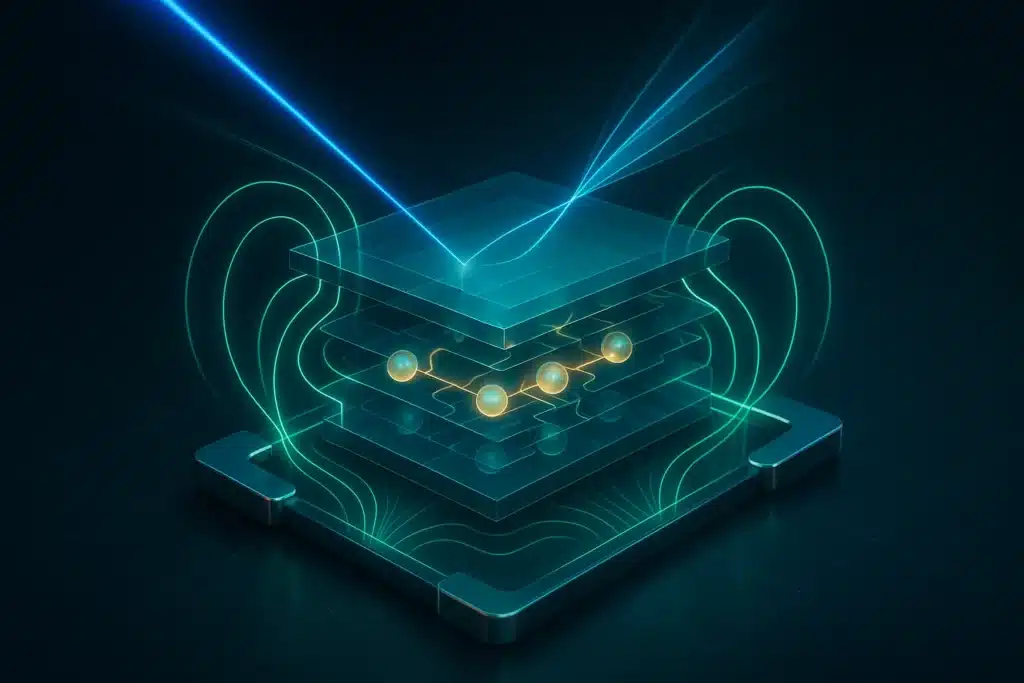
Controlling blue and ultraviolet light on a chip is becoming increasingly important for advanced chip manufacturing, high resolution microscopy, and next generation optical communication. Yet materials that can efficiently bend, guide and polarize such short wavelength light remain limited, especially in compact, chip compatible formats.

Researchers from TU Delft and Radboud University have now identified a two dimensional ferroelectric material, copper indium phosphorus sulphide or CIPS, that offers an unprecedented level of control over blue and ultraviolet light. The discovery shows that the material can be integrated onto chips and used as a powerful new building block for integrated photonics.
The compound is an atomically layered crystal with an internal electric polarization created by the displacement of copper ions. The team found that this polarization changes strongly with crystal thickness, leading to an unusual and highly tuneable refractive index. When thinned from bulk down to tens of nanometres, the material shows an unexpected change in how strongly it bends light.
Even more striking is its behaviour in the blue to ultraviolet range. Around near ultraviolet wavelengths, the material exhibits extremely large birefringence, meaning light travelling in different directions experiences dramatically different refractive indices. This allows precise control of light phase and polarization without complex nano structuring.
The researchers attribute this effect to a new light matter interaction mechanism. In the material, incoming light couples not only to electrons, but also to internal electric fields shaped by mobile copper ions. Because the ion configuration depends on thickness, the optical response can be tuned simply by selecting the crystal thickness.
Key features of the material include:
- Two dimensional ferroelectric CIPS enables strong control of blue and UV light
- Refractive index changes by nearly 25% with thickness
- Record intrinsic birefringence observed in the near UV range
- Chip compatible platform without complex nanostructuring
The team notes that this mechanism could extend beyond the compound, pointing toward a broader materials strategy where mobile ions and ferroelectric polarization are used to sculpt light, opening new possibilities for compact, tuneable UV and blue photonic devices.