Can transistors switch below the conventional power limit without sacrificing useful current? A 2D device uses quantum tunnelling to push beyond it.
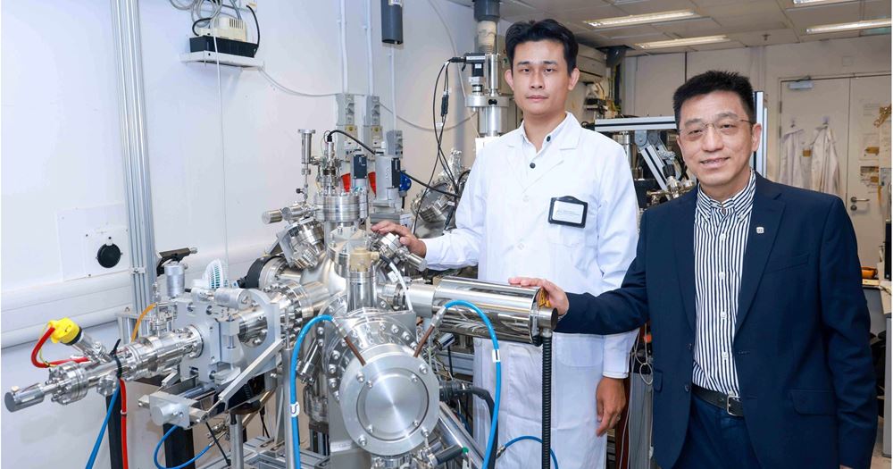
A research team led by The Hong Kong Polytechnic University has developed a tunnelling field-effect transistor (TFET) that operates below the 60mV/decade Boltzmann limit, addressing a long-standing challenge in developing lower-power integrated circuits. The research, published in Science on 27 August 2026, uses a two-dimensional bismuth-indium selenide (Bi/InSe) heterostructure to achieve quantum tunnelling-based switching.
Conventional metal-oxide-semiconductor field-effect transistor (MOSFETs) switch by thermionic emission, in which charge carriers overcome an energy barrier. At room temperature, this mechanism imposes a fundamental subthreshold swing limit of 60mV/decade, restricting how far operating voltage and power consumption can be reduced. TFETs instead use quantum tunnelling to move carriers through the barrier, potentially enabling steeper switching.
The researchers addressed a key limitation of earlier TFETs: achieving sub-Boltzmann switching while maintaining sufficient output current and a high ON/OFF ratio. They fabricated alternating ultra-thin layers of 2D bismuth (Bi) and indium selenide (InSe) using pulsed laser deposition. At this thickness, normally semimetallic bismuth becomes semiconducting, enabling band alignment that supports efficient tunnelling into InSe.
The resulting device achieved an I₆₀ of up to about 10μA/μm and a current-switching ratio exceeding 10⁷. Its subthreshold swing remained below the 60mV/decade thermionic limit across six orders of magnitude of current switching. At room temperature, it operated with a gate-voltage range of just 160mV, compared with about 800mV for advanced MOSFETs.
The device also produced output currents of several μA/μm, which the researchers say is important for driving multiple downstream logic gates and reducing circuit delay. The transistor was demonstrated on standard centimetre-scale silicon substrates, while the study showed that pulsed laser deposition could support precise, wafer-scale fabrication of the 2D materials.