
Sensor is set to enhance precision manufacturing, delivering micrometre-level point-cloud data, ultra-fast frame rates and advanced HDR imaging for demanding electronics, battery and PCB production lines.
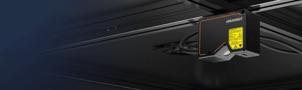
A new 3D laser profiling sensor has entered the Indian industrial automation market, aiming squarely at manufacturers in consumer electronics, lithium battery production and PCB assembly. The system by Hikrobot is built on laser triangulation and is designed to deliver real-time, micrometre-level point-cloud data for demanding inline inspection environments.

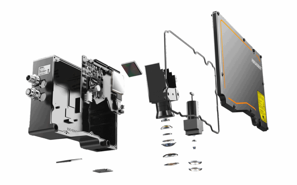
At the core of the sensor is a 405 nm blue-light module paired with a large-iris lens and a high dynamic-range imaging sensor. This combination allows the device to extract contour lines from complex surfaces with high clarity, even when reflectivity varies across the scanned object. A specialised Scheimpflug optical design maintains image sharpness across the full field of view, a requirement for high-speed factory lines where focus drift can compromise accuracy. The key features are:
- Micrometre-level 3D point-cloud, depth and intensity data in real time
- 405 nm blue-light laser with high-MTF large-iris optics for sharper contour extraction
- Frame rates up to 49 kHz with onboard high-speed processing
- Subpixel super-resolution accuracy down to 0.05 pixels
- Multi-exposure fusion, single-frame HDR and built-in filtering for complex reflectivity scenes
The system incorporates onboard computing to offload processing from external controllers. This built-in high-speed processing unit supports processing rates up to 19 kHz, while the high-speed acquisition chip can reach frame rates as high as 49 kHz, enabling fast motion scenarios typical of consumer electronics assembly or battery cell production lines.
To enhance measurement reliability, the sensor employs a centre-point extraction algorithm combined with subpixel super-resolution, pushing extraction accuracy down to 0.05 pixels. Additional features include single-frame HDR, multi-exposure fusion and optical halo suppression tools engineered to handle surfaces with low reflectivity, extreme contrast or stray-light interference.
Beyond raw capture, the device integrates spatial and time-domain filtering directly into the sensor hardware. These post-processing tools allow operators to refine depth images and point-cloud data without utilising host CPU resources, making the system adaptable for integration into existing automation setups without additional compute burden.
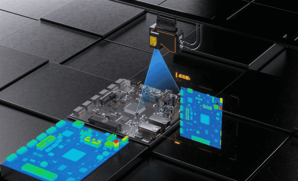
The sensor’s non-contact measurement capabilities position it for quality inspection, structural measurement and defect detection in three fast-growing manufacturing segments. In consumer electronics, it can be deployed for precise component verification. In lithium battery lines, it is suited for electrode, cell and module inspection. PCB manufacturers may use it for trace, solder and substrate evaluation where even micrometre-scale deviations can impact yield.