What if AI could design RF chips no engineer would ever imagine? The results look unusual, but some deliver performance that rivals or exceeds conventional designs.
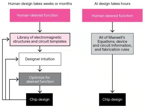
Artificial intelligence (AI) is beginning to redesign one of the most complex parts of electronics engineering by creating radio-frequency (RF) chip layouts that human engineers would be unlikely to invent. Researchers at Princeton University have developed an AI-based design framework that automatically generates radio-frequency integrated circuit (RFIC) layouts from performance targets, reducing the traditional trial-and-error design process that relies on repeated electromagnetic (EM) simulations. The researchers demonstrated the approach on fabricated millimetre-wave wireless circuits, where the AI-generated layouts matched or, in some cases, outperformed designs created by experienced RF engineers.

For decades, RF chip design has been regarded as a craft that relies on years of engineering experience and intuition. The Princeton team, led by Dr Kaushik Sengupta, Professor at Princeton University, used reinforcement learning, inverse design, and diffusion models to automate much of this process.
“RF design has long been considered a ‘dark art’ because even small layout changes can dramatically affect electromagnetic behaviour,” said Dr Kaushik Sengupta. “Our goal is to allow designers to specify the desired performance while AI explores the enormous layout space to find solutions that humans might never imagine.”
Instead of manually adjusting circuit geometries and validating each iteration through computationally intensive EM simulations, engineers only need to specify electrical requirements such as operating frequency, bandwidth, gain, or power efficiency. The AI then generates RF layouts from scratch that satisfy those targets without relying on a human-designed template. The framework does not replace circuit designers entirely. Engineers still define the circuit architecture and electrical topology, while the AI focuses on optimising the physical layout that determines electromagnetic performance.
Designing RF Chips Backwards
Unlike conventional RF design, where engineers create a layout first and then evaluate its performance, the new approach works in reverse. Starting from the required RF characteristics, the AI identifies geometries that meet the desired specifications. By learning from large numbers of EM simulation results, it can predict circuit behaviour without running a full simulation for every design iteration, allowing thousands of possible layouts to be explored in a much shorter time. Rather than memorising existing layouts, the AI learns the relationship between physical geometry and electromagnetic behaviour, enabling it to predict how entirely new layouts are likely to perform.
One of the biggest benefits is faster development. Conventional RFIC design can take weeks or even months because every layout modification requires fresh EM simulations and repeated optimisation. Rather than eliminating simulations, the AI helps identify the most promising layouts before final verification, enabling designers to evaluate many more design options while significantly shortening development cycles.
Why the Layouts Look Unusual
The layouts produced by the AI often look very different from conventional RF circuits. Many resemble QR codes, maze-like patterns, or irregular geometric structures rather than the symmetrical layouts typically created by engineers. These shapes are not generated for appearance but because they deliver the required electromagnetic behaviour. Every bend, gap, and metal structure is optimised to improve performance metrics such as efficiency, bandwidth, gain, signal integrity, and power consumption within the specified design constraints.
RF circuits are particularly suited to AI because even very small geometric changes can significantly affect electromagnetic behaviour. With millions of possible layout combinations, manually exploring every option is practically impossible. Unlike human designers, who naturally rely on years of experience and intuition, AI is not constrained by conventional design practices and can explore unconventional regions of the design space.
The researchers also developed a controllable design framework that lets engineers balance performance with interpretability. One mode generates highly unconventional layouts for maximum optimisation, while another produces layouts that more closely resemble traditional RF designs, making them easier to analyse, debug, and validate. This allows engineers to choose between maximum performance and layouts that are easier to understand and verify.
The same design philosophy is also being applied to antennae, where AI explores entirely new geometries to achieve the required electromagnetic performance instead of relying solely on established design rules.
Towards Faster Wireless Hardware Development
Researchers believe AI-assisted RF design could speed up the development of hardware for 5G, 6G, satellite communications, radar, autonomous systems, and other wireless applications. However, AI-generated layouts must still satisfy manufacturing constraints, process-design rules, and reliability requirements before they can be fabricated. As a result, the technology is expected to complement existing electronic design automation (EDA) tools rather than replace RF engineers.
The work has also sparked discussion among chip designers and AI researchers. Some engineers see AI as a way to automate repetitive RF layout optimization and explore a much larger design space than humans can manually evaluate. Others argue that human expertise will still be needed to define design constraints, verify results, and ensure the generated circuits are manufacturable.