


As processors become thinner with dense transistor layers, they generate heat. New ultrathin diamond layers spread heat, making GaN chips cooler.
As chips become smaller and faster, the heat they generate is becoming one of the biggest barriers to performance. With transistor densities and power demands rising, traditional cooling methods such as fans, radiators, and liquid systems can no longer keep up.
Researchers at Stanford University have developed a new way to manage this heat from inside the chip itself using ultra-thin diamond films that spread thermal energy before it becomes damaging.
The method allows the growth of a micrometre-thick polycrystalline diamond layer directly on semiconductor devices at low temperatures. This internal heat spreader helps control “hot spots,” which form when dense transistor activity traps energy in small regions. By dispersing heat evenly across the chip, the technology prevents overheating and reduces the need for large external cooling systems.
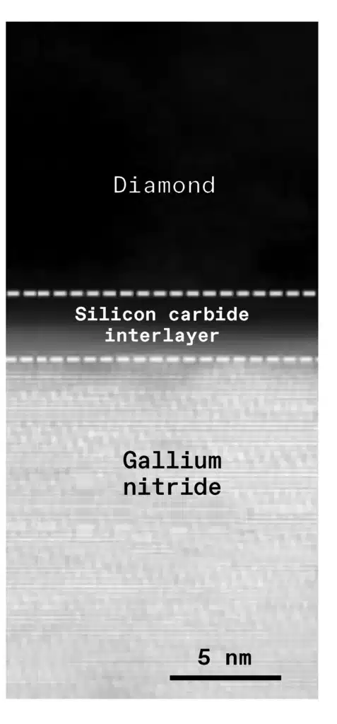
When applied to gallium-nitride radio-frequency transistors, the diamond layer reduced operating temperatures by up to 70 °C, improving stability and power handling. The researchers also found that a thin silicon-carbide interface formed naturally between the diamond and semiconductor, creating an efficient bridge for heat flow.
Diamond is one of the most thermally conductive materials, capable of carrying heat several times faster than copper while remaining electrically insulating. Until recently, diamond could be grown only at around 1,000 °C, too hot for integration with silicon or gallium-nitride devices.
The Stanford team has achieved growth at about 400 °C, low enough to protect delicate interconnects and materials used in advanced chips.
The project is being evaluated in collaboration with semiconductor manufacturers such as TSMC, Samsung, and Applied Materials. If integrated successfully, the approach could define how next-generation computing hardware manages heat as chip designs continue to scale in power and density.