
Researchers in China have developed a cutting-edge wafer-scale method to transfer 2D semiconductors like graphene with minimal defects, paving the way for high-performance, low-power electronic and optoelectronic devices.
A breakthrough in two-dimensional (2D) semiconductor integration could reshape the future of electronic device manufacturing. Researchers from Peking University, the Beijing Graphene Institute, and other Chinese institutes have unveiled a novel method to transfer 2D semiconductors with minimal defects, paving the way for smaller, more powerful electronics.

The study introduces a wafer-scale process for integrating 2D semiconductors with dielectric materials—key insulators used to regulate electrical flow in devices. Traditional transfer methods often rely on polymer supports, which introduce contaminants and defects that compromise performance. In contrast, this new technique preserves the pristine properties of graphene and enhances interface cleanliness.
“Our goal was to overcome the limitations of conventional transfer techniques by ensuring a clean, stress-free integration process,” said Zhongfan Liu, Li Lin, and Yanfeng Zhang, the paper’s corresponding authors.
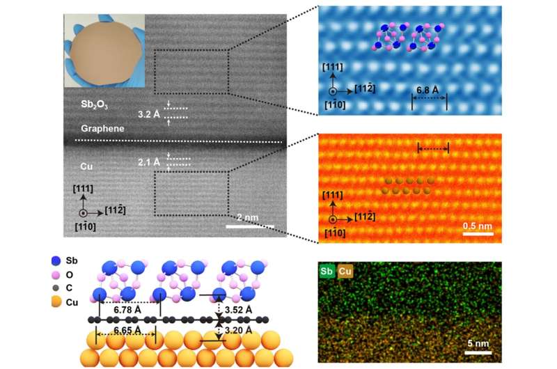
The team focused on antimony oxide (Sb₂O₃), a single-crystal dielectric. They deposited it on graphene grown on a Cu(111) surface via vacuum thermal evaporation. A water-ethanol pretreatment on the copper substrate helped reduce adhesion, simplifying the transfer process. The Sb₂O₃ layer not only enabled the transfer but also served as a protective encapsulation, guarding against mechanical and chemical damage.
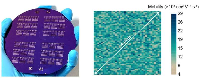
This method allowed for the successful transfer of an intact 4-inch graphene wafer with preserved electrical properties, boasting an average carrier mobility of ~14,000 cm²V⁻¹s⁻¹. The process delivered high uniformity and long-term stability, with minimal degradation over time.
Looking ahead, the researchers aim to expand their technique to 3D integration. “We’re now working on stacking and aligning 2D materials to build multi-layered, high-performance systems,” said Lin. The team’s work could soon enable scalable production of low-power, high-efficiency microelectronics and optoelectronics.This development marks a significant step toward harnessing the full potential of 2D materials in next-gen devices.