


Electronics waste energy when handling light and electricity. A new material helps reduce this loss and improve system performance.
Modern electronic devices lose a large amount of energy while switching signals between electricity and light. This limits speed, increases power use, and creates heat, especially in high-performance systems such as computer processors, data centers, and medical imaging equipment. To solve this, scientists at the University of Edinburgh, UK have developed a new semiconductor material that can move energy between light and electricity more efficiently, helping devices work faster while using less power.
The technology is aimed at scientists and engineers working on optoelectronic systems, where electrical and optical signals must operate together. These include processors, optical interconnects inside data centers, and imaging systems used in healthcare. In such systems, inefficient light absorption and emission lead to energy waste and performance limits. The new material improves these processes, allowing more effective signal conversion with lower energy loss.
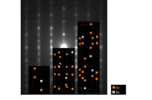
The material is based on an alloy of germanium and tin. Unlike commonly used silicon-based semiconductors, this alloy can absorb and emit light much more effectively. This enables faster conversion of light into electrical energy and electrical energy back into light, which is essential for high-speed optoelectronic devices. Earlier studies suggested that germanium–tin alloys could, in theory, work as highly efficient semiconductors, but producing them in practice was considered nearly impossible.
The main challenge was that germanium and tin do not normally react with each other under standard conditions. This prevented the formation of stable alloys suitable for electronic use. To overcome this, researchers developed a method using extreme temperature and pressure. They heated mixtures of germanium and tin to temperatures above 1200°C and applied pressures up to 10 gigapascals, around 100 times greater than the pressure at the bottom of the Mariana Trench.
This process allowed the team to create not just a single compound, but an entire class of stable germanium–tin semiconductors. These materials remain stable and functional at normal room temperature and pressure, making them suitable for real-world electronic and optoelectronic devices. The resulting alloys act as efficient semiconductors, enabling improved energy transfer between light and electricity.
