


A method spots invisible defects in semiconductors with ~1,000× greater sensitivity, a potential game-changer for chip quality and reliability.
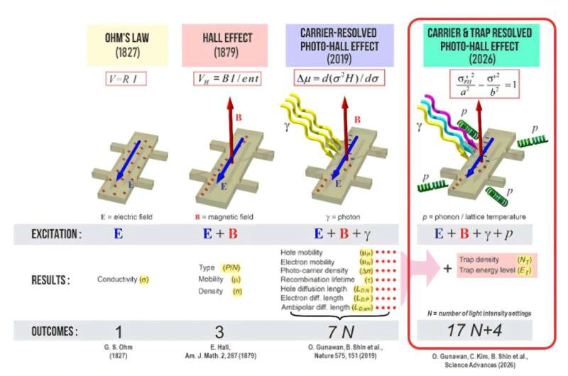
A team from KAIST and IBM has unveiled a semiconductor analysis technique that unearths so-called “hidden defects” inside electronic materials with about 1,000 times greater sensitivity than conventional methods, a leap that could reshape how chips are evaluated and optimized. At the heart of modern electronics, from memory chips to solar cells, tiny imperfections called electronic traps can capture charge carriers and disrupt normal current flow. These traps often evade standard diagnostics, causing unexplained leakage, performance loss, and reliability issues. Accurately quantifying such defects has long been a challenge for both fab engineers and materials scientists.

The new approach enhances traditional Hall effect measurements, a staple in semiconductor characterization by introducing controlled light illumination and temperature variation during the test. That lets researchers watch how electrons transition from being trapped to freely moving as illumination ramps up, enabling precise measurement of trap density and behavior in a single run.
Beyond counting traps, the technique also simultaneously captures key charge-transport parameters like carrier mobility and lifetime. That dual insight from one measurement marks a significant efficiency gain over existing defect analysis tools, which often require multiple, separate experiments to gather comparable data.
In initial trials, the team validated the method using silicon, the workhorse of the semiconductor industry and then extended it to perovskite materials, which are gaining traction in next-generation solar cells. In both cases, ultra-small quantities of previously invisible traps were detected, demonstrating the method’s enhanced sensitivity.
Researchers believe this capability could help designers and process engineers pinpoint defect sources earlier in development cycles, potentially speeding up optimization, improving yields, and boosting the performance and lifetime of devices ranging from memory chips to emerging energy technologies. The work points to a broader shift in semiconductor diagnostics where hidden loss mechanisms are no longer blind spots but quantifiable data that engineers can act on. If adopted in fabs and research labs, this enhanced analysis could reduce costly guesswork in defect mitigation and support the next wave of high-performance electronics.
