


A new cryogenic plasma etching technique developed by Japanese researchers dramatically accelerates semiconductor fabrication while cutting environmental impact, offering a potential breakthrough for advanced electronics and 3D chip architectures.
Researchers from Nagoya University and Tokyo Electron Miyagi Ltd. have developed a semiconductor etching process that boosts etch rates up to five times compared with conventional methods, potentially transforming chip manufacturing throughput for advanced devices such as gate-all-around (GAA) transistors and 3D NAND flash memory.
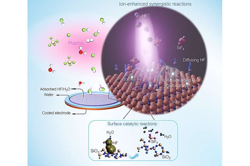
The advancement centers on a plasma etching technique using hydrogen fluoride (HF) at extremely low temperatures (~ −60 °C). Unlike traditional fluorocarbon etching gases which contribute significantly to global warming HF has a much lower global warming potential, offering both performance and environmental benefits.
Chipmakers face increasing difficulty as devices shrink and 3D architectures become more complex. Etching the process that removes material to form circuit patterns must deliver reactive chemicals deeply into high-aspect-ratio structures. Conventional reactive ion etching struggles here, slowing throughput and increasing manufacturing costs.
By cooling substrates and exposing them to HF plasma, the team found that water (H₂O) formed during the reaction adsorbs onto the surface and acts as a catalyst, lowering the activation energy required for etching. This creates a self-catalytic cycle in which HF and H₂O synergize to accelerate etch rates dramatically. Initial experiments showed that the new mechanism achieves etching throughput roughly 100 × greater than standard room-temperature, low-ion-energy conditions. The process also cuts carbon emissions tied to etching by eliminating the use of high-GWP fluorocarbon gases.
The research detailed in the Chemical Engineering Journal moves beyond laboratory proof-of-concept toward real-world manufacturing environments. By working with a major equipment maker, the team aims to integrate the process into production lines and explore broader applications across semiconductor fabrication. If scaled successfully, this cryogenic HF plasma etching technology could help address bottlenecks in next-generation chip production while reducing energy use and environmental impact.
