
Researchers use freezing technology to find how micro-sized particles cause defects in the chip-making process and design better methods to prevent them.
One of the biggest challenges in semiconductor fabrication is preventing microscopic defects that form during the lithography process. Even a particle a few nanometres wide can disrupt a circuit and render an entire chip unusable.

At advanced production nodes below 5 nanometres, such defects can lead to significant yield losses, making it critical to understand precisely how and why they occur.
Researchers in China have developed a cryogenic imaging technique that allows them to observe these defects as they form. The method uses cryo-electron tomography (cryo-ET) to freeze the chemical reactions involved in lithography and visualise them in three dimensions.
This technique, adapted from biological imaging, enables direct observation of the behaviour of photoresist materials during chip pattern development.
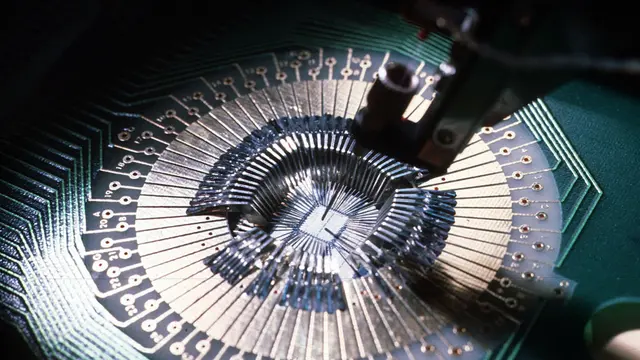
In conventional lithography, a light-sensitive liquid called photoresist is applied to a silicon wafer and exposed to ultraviolet light through a patterned mask. The exposed areas dissolve during chemical development, leaving behind a stencil that defines the circuit layout.
However, during this process, some of the dissolved materials clump together into nanoparticles. These particles can reattach to the wafer surface, creating electrical bridges or breaks that cause chip failure.
Using cryo-ET, the researchers froze the developer liquid at -175°C immediately after exposure, preserving its chemical state for imaging. The 3D analysis revealed that photoresist polymers form tangled clusters through weak molecular interactions and that many of these polymers fail to dissolve completely. They remain at the surface and redeposit during the rinsing process.
Based on these findings, the team refined the process by slightly raising the post-exposure bake temperature to reduce polymer tangling and modifying the rinse flow to sweep away surface particles. Testing on 12-inch wafers showed a 99% drop in lithography defects, offering a clearer path toward stable and high-yield semiconductor production.