


Researchers demonstrate low temperature silicon stacking that enables dense 3D chips, promising higher performance, lower power consumption and scalability.
Researchers at the University of Illinois have developed a low temperature silicon stacking technique that could accelerate the development of high density three dimensional semiconductor chips.
The breakthrough enables high performance silicon transistors to be sequentially stacked directly on top of one another, creating monolithic 3D integrated circuits. The approach addresses one of the biggest challenges in advanced chip manufacturing: building multiple layers of silicon devices without damaging the underlying circuitry through excessive heat.
Traditional chip scaling is approaching physical limits as transistors shrink to atomic dimensions. Vertical integration offers an alternative path by increasing transistor density through stacking rather than further miniaturisation. This can improve performance, reduce power consumption, and shorten communication paths between circuit blocks.
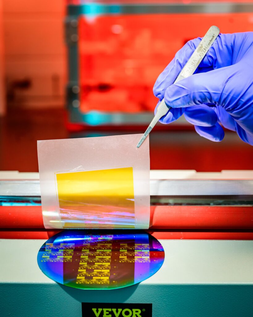
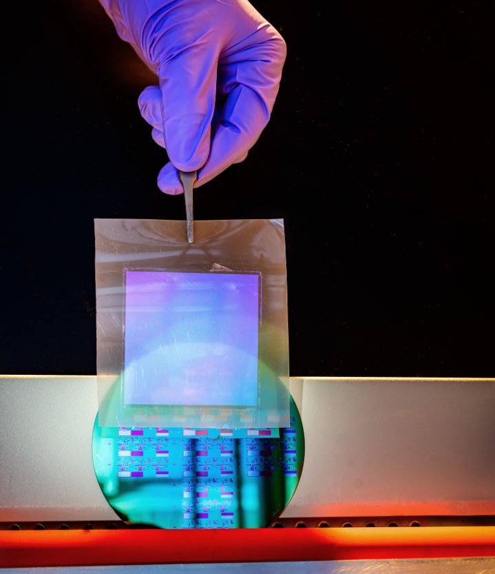
The new process uses ultrathin single crystalline silicon nanomembranes that are transferred onto completed circuit layers at temperatures below 200°C, well within the thermal limits required for monolithic 3D integration. The researchers also adopted junctionless transistor designs to eliminate high temperature doping steps typically needed during semiconductor fabrication.
Using the technique, the team successfully fabricated three stacked silicon layers containing 625 transistors each, achieving device yields of up to 100%. The transistors delivered performance comparable to conventional silicon devices manufactured using significantly higher temperature processes.
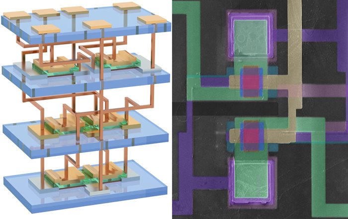
The researchers also demonstrated vertically integrated logic circuits and static random access memory cells using metal interconnections between layers. The process is designed to support additional stacking layers, potentially enabling future processors, AI accelerators, and memory devices with substantially higher computing density.
Qing Cao, Associate Professor of Materials Science and Engineering at the University of Illinois, says, “For the first time, we have met the thermal budget of monolithic 3D integration using standard single crystalline silicon and delivered unprecedented performance.”