




A new atomic layer deposition technique grows crystal-aligned tellurium films at just 150°C, enabling high-quality semiconductor devices for AI chips, optoelectronics and ultra-low-power electronics without damaging underlying materials.
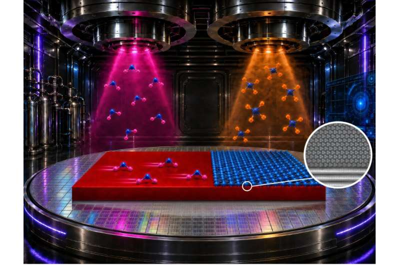
Researchers at the Korea Advanced Institute of Science and Technology (KAIST) have developed a low-temperature semiconductor fabrication technique that enables crystal-aligned tellurium (Te) thin films to be grown on two-dimensional van der Waals materials using atomic layer deposition (ALD). Operating at just 150°C, the process could accelerate the development of next-generation AI chips, ultra-low-power electronics and advanced optoelectronic devices by preserving delicate semiconductor interfaces while delivering high-quality epitaxial films.
The technology addresses a longstanding challenge in semiconductor manufacturing. Van der Waals materials such as tungsten diselenide (WSe₂), molybdenum disulfide (MoS₂) and rhenium diselenide (ReSe₂) are considered promising building blocks for future electronic devices because they can be stacked into atomically clean heterostructures. However, their chemically inert surfaces make it difficult to deposit new semiconductor layers in an ordered orientation, especially at low temperatures where precursor atoms tend to nucleate randomly, degrading electrical performance.
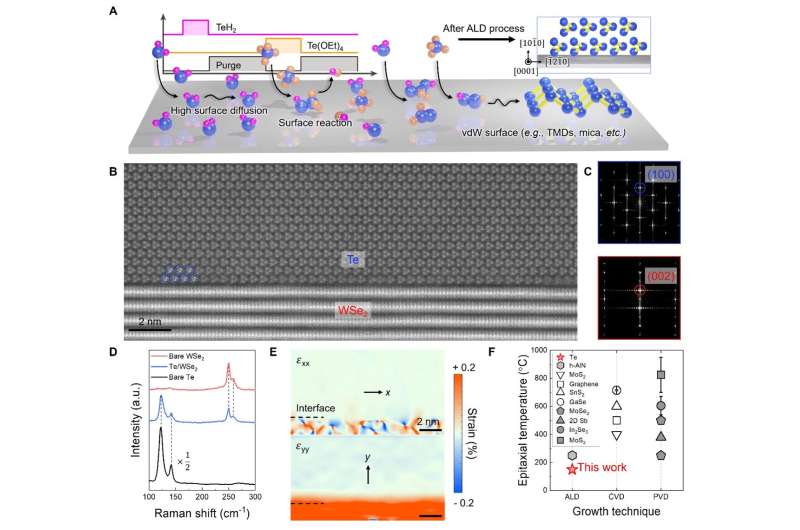
To overcome this limitation, the researchers developed a diffusion-steered epitaxial ALD process. Instead of allowing precursor molecules to attach wherever they land, the technique enables tellurium-containing precursor molecules to diffuse across the surface until they reach energetically favourable atomic sites. This controlled surface migration results in uniformly aligned epitaxial crystal growth that follows the underlying material’s lattice structure, producing high-quality semiconductor films while maintaining pristine interfaces.
Unlike conventional epitaxial growth techniques that often require significantly higher temperatures, the new method achieves crystal alignment at 150°C, making it compatible with temperature-sensitive semiconductor stacks and heterogeneous integration. Electron microscopy and structural analysis confirmed consistent crystallographic orientation and minimal interfacial distortion between the deposited tellurium film and the underlying two-dimensional material.
The team demonstrated that the approach is versatile by successfully growing aligned tellurium films on multiple van der Waals substrates, including WSe₂, MoS₂, ReSe₂ and mica. The resulting films were further used to fabricate functional transistors and optoelectronic devices, confirming that the process extends beyond material synthesis to practical semiconductor device manufacturing.
Tellurium is an attractive semiconductor for future electronics because of its highly anisotropic electrical conductivity and favourable optical properties, making it suitable for photodetectors, light-emitting diodes (LEDs) and other optoelectronic components. By combining precise crystal alignment with low-temperature processing, the new technique offers a scalable manufacturing route for integrating diverse semiconductor materials onto a single chip without compromising material quality.
The researchers believe the process could become an important manufacturing platform for heterogeneous semiconductor integration, enabling more energy-efficient AI processors, advanced photonic devices and future low-power electronic systems that rely on high-quality two-dimensional semiconductor architectures.

