


New motion-assisted image sensor combines MEMS actuation with conventional pixels to deliver ultra-high-resolution imaging, offering a fresh path beyond shrinking pixel sizes in smartphones, cameras, and medical devices.
A new image sensor architecture could reshape the future of electronics imaging by solving one of the industry’s toughest hardware bottlenecks: pixel miniaturization. Researchers at Tsinghua University have developed a motion-enhanced sensor that captures ultra-high-resolution images without relying solely on ever-smaller pixels.

For years, manufacturers have boosted camera resolution by packing more pixels into the same chip area. But as pixels shrink, they collect less light, reducing image quality, sensitivity, and dynamic range. This physical limitation has become a growing challenge for smartphone cameras, compact imaging modules, and precision medical devices.
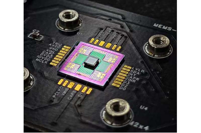
The new approach integrates a microelectromechanical systems (MEMS) actuator directly with a digital image sensor. Instead of depending only on static pixel density, the MEMS structure moves the sensor in controlled microscopic steps while multiple images are captured. These frames are then combined computationally to reconstruct a much higher-resolution final image.
This hybrid hardware-software design allows manufacturers to improve resolution while preserving larger pixel sizes that are better for low-light performance and signal quality. In practical terms, it may help electronics brands deliver sharper smartphone cameras without sacrificing night photography or sensor efficiency.
The technology could also benefit industrial inspection systems, digital microscopes, machine vision platforms, and medical imaging tools where ultra-fine detail is critical. Because the innovation builds on existing digital sensor technology, it may offer a more scalable route than redesigning semiconductor pixel structures from scratch.
For the electronics sector, the breakthrough highlights a broader trend: future performance gains may increasingly come from combining MEMS motion control, embedded processing, and computational imaging rather than traditional silicon scaling alone.
If commercialized successfully, motion-assisted sensors could become a key differentiator in next-generation cameras, smart devices, robotics, and healthcare electronics—especially as demand rises for compact systems that capture sharper images in smaller form factors.
