


Using an electrode and gate design, the device achieves record responsivity without doping—paving the way for battery-free sensors in wearables, IoT, and next-gen electronics.
A research team at the Korea Advanced Institute of Science and Technology (KAIST) has unveiled the world’s most sensitive self-powered photodetector—achieving performance levels 20 times higher than existing devices and operating without an external power supply as long as light is present. The advancement overcomes long-standing challenges in semiconductor design. Conventional silicon photodetectors suffer from low light responsivity, while ultrathin two-dimensional semiconductors such as molybdenum disulfide (MoS₂) are difficult to dope without damaging their structure—making it nearly impossible to realize high-performance PN junctions.

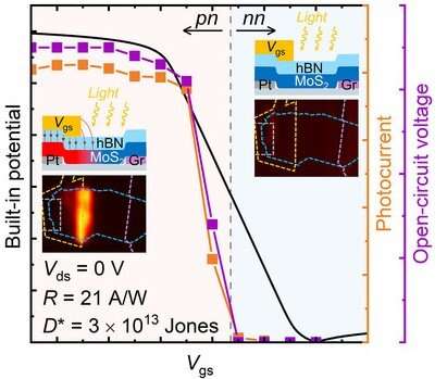
KAIST’s team, led by Professor Kayoung Lee, bypassed the need for doping by introducing two innovations: a van der Waals bottom electrode and a partial gate structure. This device architecture enables the creation of an effective PN junction—a critical element in photodetectors and solar cells—without altering the fragile atomic lattice of MoS₂.
The partial gate design selectively applies an electrical signal to different regions of the semiconductor, allowing one side to mimic p-type and the other n-type behavior. Meanwhile, the van der Waals electrode attaches gently using weak atomic forces rather than harsh chemical bonds, preserving structural integrity while maximizing electrical sensitivity.
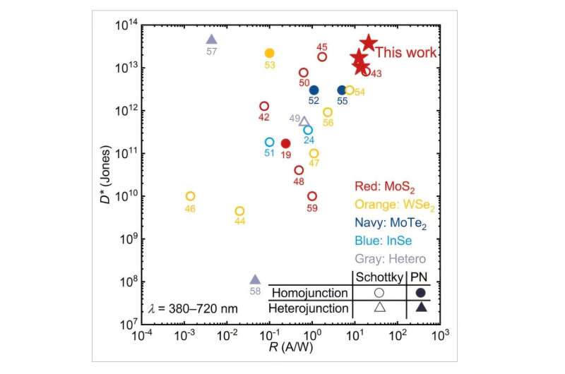
This structural stability translated into unprecedented performance. The device demonstrated a responsivity of over 21 A/W, exceeding conventional powered photodetectors by more than 20-fold, silicon-based self-powered sensors by tenfold, and MoS₂-based devices by more than double. Crucially, it operates without an external power supply, enabling real-world deployment in wearables, biosignal monitoring, IoT sensors, autonomous vehicles, and robotics.
Professor Lee noted: “We achieved a level of sensitivity unimaginable in silicon sensors. Despite the doping limitations of two-dimensional semiconductors, we implemented a PN junction that controls electrical flow without damaging the material.” Beyond sensing, the innovation could enable miniaturization and self-powered operation in next-generation electronics, from smartphones to precision biomedical devices. By solving the doping barrier, KAIST has unlocked a path toward stable, energy-efficient photodetectors—positioning two-dimensional semiconductors as a cornerstone of future optoelectronics.
